
by James E. Carroll
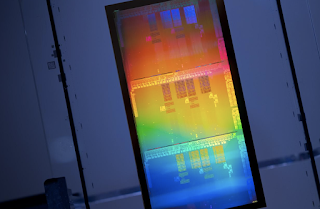
The newly established Intel Foundry Services (IFS) announced several initiatives to accelerate its entrance into the semiconductor fabrication market: a $1 billion investment fund, support for Arm and RISC-V in addition to x86, and pioneering work with chiplet architecture based on 3D packaging technology.
The new $1 billion investment fund has three aims:
- Equity investments in disruptive startups.
- Strategic investments to accelerate partner scale-up.
- Ecosystem investments to develop disruptive capabilities supporting IFS customers.
IFS confirmed that it will support multiple instruction set architectures (ISAs), spanning x86, Arm and RISC-V, making it the only foundry to offer IP optimized for all three of the industry’s leading ISAs.

The company sees strong demand from foundry customers for RISC-V and, to this end, Intel is planning investments and offerings for RISC-V. Partners in the RISC-V ecosystem include Andes Technology, Esperanto Technologies, SiFive and Ventana Micro Systems. IFS plans to offer a range of validated RISC-V IP cores, performance-optimized for different market segments. IFS will optimize IP for Intel process technologies to ensure that RISC-V runs best on IFS silicon across all types of cores, from embedded to high-performance. Three types of RISC-V offerings will be made available:
- Partner products manufactured on IFS technologies.
- RISC-V cores licensed as differentiated IP.
- Chiplet building blocks based on RISC-V, leveraging advanced packaging and high-speed chip-to-chip interfaces.
IFS also plans to sponsor an open-source RISC-V software development platform and s joining RISC-V International, a global nonprofit organization supporting the free and open RISC-V instruction set architecture and extensions.
IFS is making a major push into system-on-package architectures with an Open Chiplet Platform designed to leverage advanced 3D packaging technologies. The idea is to partition complex semiconductors into modular blocks or “chiplets.” Each block is customized for a particular function, providing designers incredible flexibility to mix and match the best IP and process technologies for the product application. Intel believes the data center market will be one of the first to adopt modular architectures. Closely integrating accelerator chiplets in the same package as a data center CPU enables significantly higher performance and reduced power compared to placing accelerator cards near CPU boards. The Open Chiplet Platform is being developed with leading cloud service providers. Intel is also partnering to develop an open standard for a die-to-die interconnect that allows chiplets to communicate with each other at high speeds.
In addition, Intel Foundry Services (IFS) today launched an Accelerator ecosystem to to spur collaboration with electronic design automation (EDA), intellectual property (IP) and design services. The IFS Accelerator provides a comprehensive suite of tools for customers:
The most powerful and validated EDA solutions optimized for Intel’s leadership technology and manufacturing, covering the full spectrum from concept to high-volume silicon production.
A comprehensive, silicon-verified, and Intel process-specific IP portfolio, including standard cell libraries, embedded memories, general purpose I/Os, analog IP and interface IP.
Design services partners that allow customers to focus on creating unique product ideas, assigning implementation tasks to rigorously trained designers well-versed on Intel technology.
The IFS Accelerator includes 17 founding partner companie as well as a broad library of IP offerings from a range of partners.
EDA Alliance: Ansys, Cadence, Siemens EDA, Synopsys
IP Alliance: Alphawave, Analog Bits, Andes, Arm, Cadence, eMemory, M31, SiFive, Silicon Creations, Synopsys, Vidatronic
Design Services Alliance: Capgemini, Tech Mahindra, Wipro

“Intel is an innovation powerhouse, but we know that not all good ideas originate from within our four walls,” said Randhir Thakur, president of Intel Foundry Services. “Innovation thrives in open and collaborative environments. This $1 billion fund in partnership with Intel Capital – a recognized leader in venture capital investing – will marshal the full resources of Intel to drive innovation in the foundry ecosystem.”
“Foundry customers are rapidly embracing a modular design approach to differentiate their products and accelerate time to market. Intel Foundry Services is well-positioned to lead this major industry inflection. With our new investment fund and open chiplet platform, we can help drive the ecosystem to develop disruptive technologies across the full spectrum of chip architectures,” said Pat Gelsinger, Intel CEO.
Saf Yeboah, senior vice president and chief strategy officer at Intel, said: “Intel Capital’s history and expertise are rooted in chips. Over the last 30 years, we have invested over $5 billion into 120 companies supporting the semiconductor manufacturing ecosystem, from the materials coming out of the ground to the software tools used to implement a design. Our investments, which range from pathfinding bets into early-stage companies to deeply strategic and collaborative investments, drive innovation across architecture, IP, materials, equipment and design.”
Intel expands its manufacturing plans
Intel will invest more than $20 billion in the construction of two new fabs in Ohio. The initial phase of the project is expected to create 3,000 Intel jobs and 7,000 construction jobs over the course of the build. Air Products, Applied Materials, LAM Research and Ultra Clean Technology will establish a physical presence in the region. Initial production is targetted for 2025.
In a press conference, Gelsinger said the new facilities will produced advanced chip designs at 2nm and below.
“The impact of this mega-site investment will be profound,” said Keyvan Esfarjani, Intel senior vice president of Manufacturing, Supply Chain and Operations. “A semiconductor factory is not like other factories. Building this semiconductor mega-site is akin to building a small city, which brings forth a vibrant community of supporting services and suppliers. Ohio is an ideal location for Intel’s U.S. expansion because of its access to top talent, robust existing infrastructure, and long history as a manufacturing powerhouse. The scope and pace of Intel’s expansion in Ohio, however, will depend heavily on funding from the CHIPS Act.”
https://www.intel.com/content/www/us/en/newsroom/resources/global-manufacturing.html#gs.mt8qf9
Intel breaks ground on $20 billion fabs in AZ


