Monday, April 29, 2024

NTT develops fabrication tech for flexible optical networks

NTT has developed a fabrication technology that allows various types of optical fibers to branch and merge without causing communication interruption.

Worldwide, optical fibers come in different refractive index distributions and exhibit varied propagation characteristics (known as effective refractive index). Traditional methods of branching these fibers required matching the effective refractive index between the source and destination fibers, necessitating knowledge of the branch source's refractive index and preparation of a suitable branch fiber. This process often interrupted service at the branch source. 

To overcome this challenge, NTT says there's a need to develop technology allowing fiber branching during communication, independent of their effective refractive index.

NTT developed a method to make branched optical fibers with varying core diameters. This variation affects the effective refractive index, allowing these fibers to have different effective refractive indices. With this structure, branching optical fibers becomes possible regardless of the source fiber's effective refractive index. NTT's breakthrough in fabricating these fibers marks a global first, significantly expanding the types of fibers that can be branched compared to traditional ones. This advancement enables the branching and merging of all fibers meeting international standards commonly used in optical access networks.


https://group.ntt/en/newsrelease/2024/04/24/240424b.html

false

Thintronics raises $23M for unified insulator

Thintronics, a start-up based in Berkeley, California, raised $23 million in Series A funding for its development of electronic materials for high-performance insulators for emerging AI datacenter, networking, and RF/millimeter-wave (mmW) applications.

The funding was led by Maverick Capital and Translink Capital. Series A funding will support commercialization of a novel insulator platform.

The company was founded on the idea that conventional assumptions guiding insulator material development limited the capacity of the industry to innovate. Thintronics says its suite of high-performance materials display electrical and mechanical characteristics that far outpace the state of the art. 

Thintronics’ CEO Stefan Pastine emphasizes that "the interconnect insulator is foundational to modern electronics; however, it has yet to be optimized to operate near the theoretical limit of insulation. Additionally, the supply chain is fragmented across multiple electronic architectures. It is our vision to optimize the insulator and unify it across the fabric."

To satisfy this growing demand Thintronics is entering the insulator market with technologies targeting chipsets, switches, and datacenter integrators for 224G links and beyond. For CTO Tristan El Bouayadi, "The combination of superior electrical and thermo-mechanical performance allows our customers to unlock new design possibilities and new applications in Networking, AI acceleration, RF mmW communication, and Radar. Additionally, by synthesizing ultra-thin dielectric layers, Thintronics enables form factor design optimization for Consumer and Infrastructure devices and products."

https://thintronics.com/

false

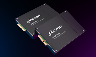
Micron awarded $6.1B in CHIPS Act funding

 Micron Technology has reached a preliminary agreement under the CHIPS and Science Act under which it will receive $6.1 billion to develop advanced memory manufacturing facilities in Idaho and New York. The total investment from Micron could reach $50 billion by 2030, supporting the creation of several leading-edge memory production plants. This includes expanding an existing facility in Boise, Idaho, and constructing two new facilities in Clay, New York.

The funding and additional incentives from state and local governments, as well as potential tax credits from the U.S. Treasury, will facilitate competitive, cutting-edge memory manufacturing in the U.S. These initiatives are expected to generate about 75,000 jobs over the next 20 years, boosting both local economies and the national economic and security landscape. The investments represent significant private financial commitments in Idaho and New York, marking a major step in enhancing U.S. semiconductor capabilities and innovation.

Micron initiated construction on its Boise fab in October of calendar year 2023. The fab will be co-located with Micron’s world-class R&D center to enhance operational efficiency, accelerate technology deployment and improve time to market for leading-edge products. The Idaho fab is expected to come online and be operational in calendar year 2025, with DRAM output starting in calendar year 2026 and ramping in line with market demand over the second half of the decade.

In New York, preliminary design, field studies and permitting applications, including NEPA, are underway for the project. Construction of the first fab is expected to begin in calendar year 2025 and to come online and contribute to output in calendar year 2028, ramping in line with market demand over the next decade.


false

SURF tests 800G link over 1,650 km fiber with Ribbon

 SURF, the collaborative organization for IT in Dutch education and research, achieved 800G over a brownfield 1,650 km fiber optic link using Ribbon Communications' optical transport platform. The trial connected research institutes including Nikhef with The Large Hadron Collider located on the CERN campus in Geneva.

The trial demonstrated a number of Ribbon's advanced transport solutions:

  • Apollo TM800_2, which uses industry-leading 5nm-140Gbaud transmission technology to deliver capacity-reach optimized 800G transport.
  • Apollo Open Optical Line Systems, which include hybrid EDFA-Raman amplifiers that maximize the capacity of SURF's brownfield G655 and G652 fiber, and have a proven ability to carry third-party vendor wavelengths.
  • NPT 2400 metro router, which is interoperable with SURF's network and delivered 2x400GbE uplinks running EVPN services on top of BGP to 8x100G ports on that network.

"We are proud to collaborate with our partner Ribbon in this successful and innovative trial, which pushes the boundaries of our current fiber and shows us what is technically possible with Ribbon's equipment," said Harold Teunissen, Director Network & Campus at SURF. "This trial signifies a crucial step forward as we gear up our network to cater to the future needs of scientific research and education in the Netherlands and beyond."

"We're excited to work with SURF to demonstrate how they can deliver advanced transport services to their research and education partners over the existing infrastructure," said Sam Bucci, COO and EVP, Ribbon. "We're proud to deliver innovative solutions that contribute to the advancement of science."

Canada's Valo Networks picks Ekinops360 WDM

Valo Networks will be deploying the Ekinops360 WDM transport platform to deliver rural broadband connectivity in Red Deer County, Alberta, Canada.

Valo Networks, launched in 2019, specializes in operating next-generation fiber-optic and wireless networks.  It is providing full turn-key service including the design, installation, commissioning, and ongoing operation of Red Deer County's new fiber optic network in the province of Alberta.  To serve Canadian communities like Red Deer County, Valo Networks created its Open Access Network (OAN) network architecture that provides scalable, accessible, and future-proof capacity that can be customized for individual communities.

Valo is building the new network using Ekinops360 WDM system, starting at 10G with the capability to scale to higher capacities as demand increases. 

https://www.ekinops.com/solutions/optical-transport