
IBM and Samsung Electronics unveiled a new class of Vertical Transport Field Effect Transistors (VTFET) - a breakthrough the companies say that could reduce energy usage by 85 percent compared to a scaled fin field-effect transistor (finFET). The design positions the transistors perpendicular to the surface of the chip with a vertical, or up-and-down, current flow. IBM says the vertical positioning allows for greater current flow with less wasted energy.
The partners have demonstrated a path to scaling beyond nanosheet, implying a path toward manufacturability and further innovation.
Research was carried out at IBM's Albany Nanotech Complex facility.
The companies also announced that Samsung will manufacture IBM's chips at the 5 nm node. These chips are anticipated to be used in IBM's own server platforms. This follows the announcement in 2018 that Samsung would manufacture IBM's 7 nm chips, which became available in the IBM Power10 family of servers earlier this year. The IBM Telum processor, also revealed earlier this year, is similarly manufactured by Samsung using IBM's designs.
Samsung Foundry targets 3nm in 2022, 2nm in 2025

IBM announces 2nm chip breakthrough
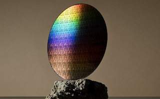
IBM unveiled a 2 nanometer semiconductor design and process breakthrough based on a new Gate-All-Around (GAA) nanosheet device architecture. The technology is implemented on a 300 millimeter (mm) wafer built at IBM Research’s semiconductor research facility in Albany, New York.

IBM Research’s Albany lab features one of the most advanced EUV lithography tools in the industry.
"The IBM innovation reflected in this new 2 nm chip is essential to the entire semiconductor and IT industry," said Darío Gil, SVP and Director of IBM Research. "It is the product of IBM's approach of taking on hard tech challenges and a demonstration of how breakthroughs can result from sustained investments and a collaborative R&D ecosystem approach."


