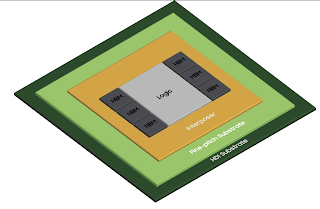
Samsung Electronics introduced Hybrid-Substrate Cube (H-Cube) technology, its latest 2.5D packaging solution specialized for semiconductors for HPC, AI, data center, and networking chips that require high-performance and large-area packaging technology.
2.5D packaging enables logic chips or high-bandwidth memory (HBM) to be placed on top of a silicon interposer in a small form factor.Samsung said its H-Cube technology features a hybrid substrate combined with a fine-pitch substrate which is capable of fine bump connection, and a High-Density Interconnection (HDI) substrate, to implement large sizes into 2.5D packaging.
“H-Cube solution, which is jointly developed with Samsung Electro-mechanics (SEMCO) and Amkor Technology, is suited to high-performance semiconductors that need to integrate a large number of silicon dies,” said Moonsoo Kang, senior vice president and Head of Foundry Market Strategy Team at Samsung Electronics. “By expanding and enriching the foundry ecosystem, we will provide various package solutions to find a breakthrough in the challenges our customers are facing.”
“In today’s environment where system integration is increasingly required and substrate supplies are constrained, Samsung Foundry and Amkor Technology have successfully co-developed H-Cube to overcome these challenges,” said JinYoung Kim, senior vice president of Global R&D Center at Amkor Technology. “This development lowers barriers to entry in the HPC/AI market and demonstrates successful collaboration and partnership between the foundry and outsourced semiconductor assembly and test (OSAT) company.”
https://www.samsungfoundry.com


