
Samsung Foundry is scheduled to start producing its customers' first 3nm-based chip designs in the first half of 2022, while its second generation of 3nm is expected in 2023.
Samsung said its first 3nm GAA process node utilizing Multi-Bridge-Channel FET (MBCFETTM) will allow up to 35 percent decrease in area, 30 percent higher performance or 50 percent lower power consumption compared to the 5nm process. In addition to power, performance, and area (PPA) improvements, as its process maturity has increased, 3nm’s logic yield is approaching a similar level to the 4nm process, which is currently in mass production.
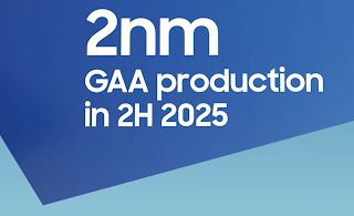
The 2nm process node with MBCFET is in the early stages of development with mass production in 2025.

“We will increase our overall production capacity and lead the most advanced technologies while taking silicon scaling a step further and continuing technological innovation by application,” said Dr. Siyoung Choi, President and Head of Foundry Business at Samsung Electronics. "Amid further digitalization prompted by the COVID-19 pandemic, our customers and partners will discover the limitless potential of silicon implementation for delivering the right technology at the right time."
Additionally, Samsung is advancing its 14nm process in order to support 3.3V high voltage or flash-type embedded MRAM (eMRAM) which enables increased write speed and density. It will be a great option for applications such as micro controller unit (MCU), IoT and wearables. Samsung’s 8nm radio frequency (RF) platform is expected to expand the company’s leadership in the 5G semiconductor market from sub-6GHz to mmWave applications.
http://news.samsung.com


