
Intel showcased a number of advancements in the field of optical interconnects, advancing its long-term ambition to bring optical I/O directly into silicon packages. During a virtual Intel Labs day presentatio, the company demonstrated advances in key technology building blocks, including with light generation, amplification, detection, modulation, complementary metal-oxide semiconductor (CMOS) interface circuits and package integration.
Key technology building blocks showcased:
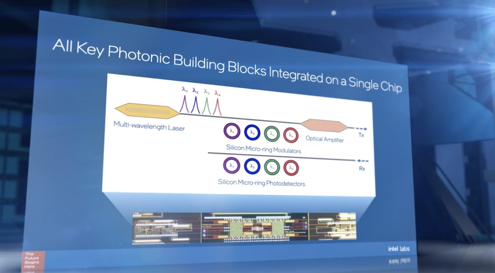
- Micro-ring modulators: Conventional silicon modulators take up too much area and are costly to place on IC packages. By developing micro-ring modulators, Intel has miniaturized the modulator by a factor of more than 1,000, thereby eliminating a key barrier to integrating silicon photonics onto a compute package.
- All-silicon photodetector: For decades, the industry has believed silicon has virtually no light detection capability in the 1.3-1.6um wavelength range. Intel showcased research that proves otherwise. Lower cost is one of the main benefits of this breakthrough.
- Integrated semiconductor optical amplifier: As the focus turns to reducing total power consumption, integrated semiconductor optical amplifiers are an indispensable technology, made possible with the same material used for the integrated laser.
- Integrated multi-wavelength lasers: Using a technique called wavelength division multiplexing, separate wavelengths can be used from the same laser to convey more data in the same beam of light. This enables additional data to be transmitted over a single fiber, increasing bandwidth density.
- Integration: By tightly integrating silicon photonics and CMOS silicon through advanced packaging techniques, we can gain three benefits: lower power, higher bandwidth and reduced pin count. Intel is the only company that has demonstrated integrated multi-wavelength lasers and semiconductor optical amplifiers, all-silicon photodetectors, and micro-ring modulators on a single technology platform tightly integrated with CMOS silicon. This research breakthrough paves the path for scaling integrated photonics.
Intel said these advancements will enable future architectures that are more disaggregated, with multiple functional blocks such as compute, memory, accelerators and peripherals spread throughout the entire network and interconnected via optical and software in high-speed and low-latency links.
“We are approaching an I/O power wall and an I/O bandwidth gap that will dramatically hinder performance scaling. The rapid progress Intel is making in integrated photonics will enable the industry to fully re-imagine data center networks and architectures that are connected by light. We have now demonstrated all of the critical optical technology building blocks on one silicon platform, tightly integrated with CMOS silicon. Our research on tightly integrating photonics with CMOS silicon can systematically eliminate barriers across cost, power and size constraints to bring the transformative power of optical interconnects to server packages,” stated James Jaussi, senior principal engineer and director of PHY Lab, Intel Labs.
Without such advancements, Intel warns the industry will soon reach the practical limits of electrical I/O performance - what it calls an "I/O power wall".


