Showing posts with label Rambus. Show all posts

Monday, October 31, 2022

Rambus posts strong Q3, exceeding guidance

Rambus posted Q3 GAAP revenue of $112.2 million, with licensing billings at $62.2 million, product at was $58.6 million, and contract and other revenue of $23.7 million. The company also generated $80 million in cash provided by operating activities in the third quarter.

“Rambus had an excellent performance in the third quarter, exceeding guidance and delivering record cash and product revenue,” said Luc Seraphin, chief executive officer of Rambus. “Our strategic focus and strong execution in data center, combined with a diverse portfolio of offerings, drive the company’s long-term profitable growth and enable consistent capital returns to our stockholders.”

Separately, Rambus extended its patent license agreement with Samsung Electronics. This substantially maintains the existing financial terms and provides Samsung with broad access to the full Rambus patent portfolio through late 2033. Other terms and details are confidential.

https://investor.rambus.com/press-releases/press-release-details/2022/Rambus-Reports-Third-Quarter-2022-Financial-Results/default.aspx

Tuesday, October 25, 2022

Rambus delivers PCIe 6.0 subsystem supporting CXL

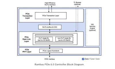
Rambus released its PCI Express (PCIe) 6.0 Interface Subsystem comprised of PHY and controller IP. 

The Rambus PCIe 6.0 Interface Subsystem delivers data rates of up to 64 Gigatransfers per second (GT/s) and has been fully optimized to meet the needs of advanced heterogenous computing architectures. Within the subsystem, the PCIe controller features an Integrity and Data Encryption (IDE) engine dedicated to protecting the PCIe links and the valuable data transferred over them. On the PHY side, full support for CXL 3.0 is available to enable chip-level solutions for cache-coherent memory sharing, expansion and pooling.

Key features of the Rambus PCIe 6.0 Interface Subsystem include:

  • Supports PCIe 6.0 specification including 64 GT/s data rate and PAM4 signaling
  • Implements low-latency Forward Error Correction (FEC) for link robustness
  • Supports fixed-sized FLITs that enable high-bandwidth efficiency
  • Backward compatible to PCIe 5.0, 4.0 and 3.0/3.1
  • State-of-the-art security with an IDE engine (controller)
  • Supports CXL 3.0 for new use models that optimize memory resources (PHY)

“The rapid advancement of AI/ML and data-intensive workloads is driving the continued evolution of data center architectures requiring ever higher levels of performance,” said Scott Houghton, general manager of Interface IP at Rambus. “The Rambus PCIe 6.0 Interface Subsystem supports the performance requirements of next-generation data centers with premier latency, power, area and security.”


Tuesday, July 19, 2022

Rambus expands its line of DDR5 memory interface chips

Rambus has expanded its DDR5 memory interface chip portfolio with the addition of the Rambus SPD (Serial Presence Detect) Hub and Temperature Sensor, complementing its Registering Clock Driver (RCD), to deliver high-performance, high-capacity memory solutions for DDR5 computing systems. Both the SPD Hub and Temperature Sensor are critical components on a memory module that sense and report important data for system configuration and thermal management. The SPD Hub is used in both server and client modules, including RDIMMs, UDIMMS and SODIMMS, and the temperature sensor is designed for server RDIMMs.

“The new performance levels of DDR5 memory place an increased premium on signal integrity and thermal management for server and client DIMMs,” said Sean Fan, chief operating officer at Rambus. “With over 30 years of memory subsystem design experience, Rambus is ideally positioned to deliver DDR5 chipset solutions which enable breakthrough bandwidth and capacity for advanced computing systems.”

Key features of the SPD Hub (SPD5118) include:
  • I2C and I3C bus serial interface support Advanced reliability features 
  • Expanded NVM space for customer-specific applications 
  • Low latency for fastest I3C bus rates 
  • Integrated temperature sensor 
  • Meets or exceeds all JEDEC DDR5 SPD Hub operational requirements (JESD300-5A) 

Key features of the Temperature Sensor (TS5110) include:
  • Precision thermal sensing I2C and I3C bus serial interface support 
  • Low latency for fastest I3C bus rates 
  • Meets or exceeds all JEDEC DDR5 Temperature Sensor operational requirements (JESD302-1.01)

https://www.rambus.com/rambus-expands-portfolio-of-ddr5-memory-interface-chips-for-data-centers-and-pcs/

Rambus samples 5600 MT/s DDR5 registering clock driver

Rambus has begun sampling its 5600 MT/s 2nd-generation registering clock driver (RCD) chip to the major DDR5 memory module (RDIMM) suppliers. This new level of performance represents a 17% increase in data rate over the first-generation 4800 MT/s Rambus DDR5 RCD. Rambus said it is able to deliver 5600 MT/s performance at lower latency and power while optimizing timing parameters for improved RDIMM margins.“The RCD is a mission-critical...


Thursday, May 5, 2022

Rambus to acquire Hardent for semiconductor design team

Rambus agreed to acquire Hardent, a professional services company specializing in electronic product design and engineering. The company, which is based in Montreal, has 20 years of semiconductor experience in silicon design, verification, compression, and Error Correction Code (ECC). Financial terms were not disclosed.

Rambus says the acquisition augments its team of engineers at Rambus and accelerates the development of CXL processing solutions for next-generation data centers. In addition, Hardent brings complementary IP and services to the Rambus Silicon IP portfolio, expanding the customer base and design wins in automotive and consumer electronic applications. 

“Driven by the demands of advanced workloads like AI/ML and the move to disaggregated data center architectures, industry momentum for CXL-based solutions continues to grow,” said Luc Seraphin, president and CEO of Rambus. “The addition of the highly-skilled Hardent design team brings key resources that will accelerate our roadmap and expand our reach to address customer needs for next-generation data center solutions.”

“The Rambus culture and track record of technology leadership is an ideal fit for Hardent,” said Simon Robin, president and founder of Hardent. “The team is looking forward to joining Rambus and is excited to be part of a global company advancing the future of data center solutions.”

https://www.rambus.com/rambus-to-acquire-hardent/

Wednesday, January 26, 2022

Rambus delivers PCIe 6.0 controller

Rambus released a PCI Express 6.0 Controller, delivering data rates up to 64 Gigatransfers per second (GT/s) for high-performance applications. In addition, the controller provides an Integrity and Data Encryption (IDE) engine that monitors and protects PCIe links against physical attacks.

“The rapid advancement of AI/ML and data-intensive workloads requires that we continue to provide higher data rate solutions with best-in-class latency, power and area,” said Sean Fan, chief operating officer at Rambus. “As the latest addition to our portfolio of industry-leading interface IP, our PCIe 6.0 Controller offers customers an easy to integrate solution that delivers both performance and security for advanced SoCs and FPGAs.”

Key features of the Rambus PCIe 6.0 Controller include:

  • Supports PCIe 6.0 specification including 64 GT/s data rate and PAM4 signaling
  • Supports fixed-sized FLITs that enable high-bandwidth efficiency
  • Implements low-latency Forward Error Correction (FEC) for link robustness
  • Internal data path size automatically scales up or down (256, 512, 1024 bits) based on max. link speed and width for reduced gate count and optimal throughput
  • Backward compatible to PCIe 5.0, 4.0 and 3.0/3.1
  • Supports Endpoint, Root-Port, Dual-Mode and Switch port configurations
  • Integrated IDE optimized for performance

https://www.rambus.com/rambus-delivers-pcie6-controller-for-next-generation-data-centers/

New PCIe 6.0 spec delivers 64 GT/s raw data rate

PCI-SIG, the organization responsible for the widely adopted PCI Express standard, officially released the PCIe 6.0 specification boasting a top raw data rate of 64 GT/s (gigatransfers per second) -- double the bandwidth and power efficiency of the PCIe 5.0 specification (32 GT/s).Applications for PCIe 6.0 are expected to include data centers, AI/ML, HPC, and defense systems.PCIe 6.0 Specification Features64 GT/s raw data rate and up to 256...


Wednesday, October 13, 2021

Rambus samples 5600 MT/s DDR5 registering clock driver

Rambus has begun sampling its 5600 MT/s 2nd-generation registering clock driver (RCD) chip to the major DDR5 memory module (RDIMM) suppliers. 

This new level of performance represents a 17% increase in data rate over the first-generation 4800 MT/s Rambus DDR5 RCD. 

Rambus said it is able to deliver 5600 MT/s performance at lower latency and power while optimizing timing parameters for improved RDIMM margins.

“The RCD is a mission-critical enabler of DDR5 server DIMMs that provide the bandwidth and capacity needed in next-generation data centers,” said Sean Fan, chief operating officer at Rambus. “Achieving the 5600 MT/s data rate is the latest demonstration of our continued leadership in DDR5 memory interface products.”

https://www.rambus.com/rambus-advances-server-memory-performance-with-the-industrys-first-5600-mt-s-ddr5-registering-clock-driver/

Wednesday, June 17, 2020

Rambus delivers 112G XSR/USR PHY on TSMC 7nm

Rambus announced the availability of its 112G XSR/USR PHY based on TSMC’s industry-leading 7nm process.

Applications for the 112G XSR/USR PHY  and chiplet architectures include next-generation 51.2 Terabit per second (Tbps) ASICs for network switches, where 112G XSR links will connect the digital switch ASIC die to CPO engines. In AI/ML and HPC SoCs, the 112G XSR PHY can be used to bridge purpose-built accelerator chiplets for natural language processing, video transcoding and image recognition. Another popular use case is the die disaggregation of large SoCs, hitting reticle size limits for manufacturable yields, into multiple smaller die connected using XSR links over organic substrate. Increasingly, these advanced applications are implemented on TSMC’s N7 process.

“This important milestone highlights Rambus’ leadership in high-speed SerDes enabling the industry’s highest value and most demanding applications,” said Hemant Dhulla, vice president and general manager of IP cores at Rambus. “At an industry-leading power efficiency of sub-picojoule per bit, and unidirectional bandwidth approaching two terabit per second per millimeter, we are very proud to offer our 112G XSR/USR solution in partnership with TSMC.”

“We’re pleased with the availability of Rambus’ PHY on our N7 process technology to address the growing market need for low-power, high-performance chiplet architectures,” said Suk Lee, senior director of the Design Infrastructure Management Division at TSMC. “Our ongoing partnership with Rambus ensures that designers can meet next-generation requirements for performance and power efficiency in computing, AI/ML and networking using TSMC’s advanced process technologies.”

https://www.rambus.com/interface-ip/serdes/112g-xsr-phy

Tuesday, November 12, 2019

Rambus announces PCI Express 5.0 interface

Rambus announced a comprehensive and optimized interface for PCI Express (PCIe) 5.0 in an advanced 7nm FinFET process, and offering backward compatibility to PCIe 4.0, 3.0 and 2.0.

The Rambus PCIe 5.0 interface solution includes both PHY and digital controller for easy SoC integration and faster time to market.

Highlights of Rambus PCIe 5.0 solution

  • Integrated and co-validated PHY and digital controller for complete interface solution
  • Built with Rambus’ industry-proven design methodology for long-reach PCIe interfaces
  • 32 GT/s bandwidth per lane with 128 GB/s bandwidth in x16 configuration
  • Backward compatible to PCIe 4.0, 3.0 and 2.0
  • Supports Compute Express Link interconnect
  • Advanced multi-tap transceiver and receiver equalization compensate for more than 36dB of insertion loss

“Our high-speed SerDes and memory interface solutions make possible amazing advancements in performance-intensive applications in AI, data center, HPC, storage and networking,” said Hemant Dhulla, vice president and general manager of IP cores at Rambus. “Now we’ve added PCIe 5 to our industry-leading portfolio of high-speed interface solutions giving chip makers another tool to unleash the power of their designs.”

Wednesday, October 30, 2019

Rambus GDDR6 Memory PHY hits 18 Gbps

The newest Rambus GDDR6 Memory PHY has achieved industry-leading 18 Gbps peak performance, roughly four-to-five times faster than current DDR4 solutions.

The Rambus GDDR6 PHY pairs with the companion GDDR6 memory controller from the recent acquisition of Northwest Logic to provide a complete and optimized memory subsystem solution.

“Memory bandwidth poses a significant obstacle for designers working on performance-intensive applications such as AI/ML,” said Hemant Dhulla, vice president and general manager of IP cores at Rambus. “With our GDDR6 18 Gbps memory subsystem, Rambus technology can unleash the power of leading-edge designs with a proven and cost-effective memory architecture.”

Benefits of the Rambus GDDR6 PHY:

  • Achieves the industry’s highest speed of up to 18 Gbps, delivering a maximum bandwidth of up to 72 GB/s
  • Complete and optimized memory subsystem solution with companion GDDR6 memory controller
  • Offers PCB and package design support – allowing customers to quickly and reliably bring their high-speed designs to production
  • Provides access to Rambus system and SI/PI experts helping ASIC designers to ensure maximized signal and power integrity for devices and systems
  • Features LabStation development environment that enables quick system bring-up, characterization and debug
  • Supports high-performance applications including networking, data center, ADAS, machine learning and AI

Wednesday, September 25, 2019

Rambus tapes out its 112G XSR SerDes PHY

Rambus taped out its 112G XSR SerDes PHY on a leading-edge 7nm process node optimized for PPA to support data center, networking, HPC, AI and ML applications.

Rambus said its 112G XSR SerDes PHY represents the latest advancement in high-speed signaling technology for die-to-die (D2D) and die-to-optical engine (D2OE) connections.

"As semiconductor markets turn towards chiplets to enable their high-performance products, chip-to-chip interconnects will be critical for maintaining high speed and signal integrity across variable physical distances," said Shane Rau, research vice president, computing semiconductors at IDC. "SerDes PHYs at advanced process nodes, like the 7nm 112G XSR, enable that speed and signal integrity."

“Our 112G XSR SerDes PHY is implemented in the leading-edge 7nm process technology, providing chip and system architects the most advanced platform for their designs,” said Hemant Dhulla, vice president and general manager of IP cores at Rambus. “We are excited to continue our tradition of delivering leading-edge IP solutions that address the systems design challenges of the most demanding applications in networking, HPC and AI.”

The Rambus 112G XSR SerDes PHY includes:

  • High-bandwidth connectivity greater than 800 Gbps per millimeter of beachfront making it ideal for D2D and D2OE interconnects in networking and HPC applications
  • Designed to provide a low-power, high-speed interface that supports chip disaggregation
  • Best-in-class architecture for power, performance, area (PPA) with approximately 1 pJ/bit or 1mW/Gbps power
  • Compliance with Open Interface Forum Common Electrical I/O Consortium (OIF-CEI) standard


Tuesday, September 3, 2019

Verimatrix to sell Silicon IP business to Rambus

Verimatrix will sell its Silicon IP and Secure Protocols (SIP) business unit to Rambus for $65 million in cash.

The SIP business unit provides intellectual property components, software toolkits and provisioning solutions to enable semiconductor manufacturers and fabless companies, device manufacturers and security software integrators to meet the critical needs for secure communication and performance acceleration, information protection and user privacy for IoT and network security markets. The business generated $22 million annual revenue.

"We are pleased to announce this exclusivity agreement to sell our Silicon IP and Secure Protocols business unit to Rambus, a premier silicon IP and chip provider,” said Amedeo D'Angelo, Chairman and CEO of Verimatrix. "This transaction ideally fits with our strategy to focus our company as a pure player in software-based security solutions. After completion, we will have the agility to fully address promising growth markets such as Entertainment, Mobile Applications and the Internet of Things. Additionally, the transaction will significantly increase our financial flexibility to seize external growth opportunities and reinforce our commitment to bringing the best value proposition to our customers.”

“The embedded security team at Verimatrix has a well-recognized and long-standing history of providing security at the heart of SoCs,” said Luc Seraphin, president and CEO of Rambus. “Their combination of products and expertise is highly complementary to our existing business and will expand our global reach for our worldwide security customer base.”

Tuesday, June 4, 2019

Achronix next-gen FPGAs leverage Rambus GDDR6 PHY

Achronix Semiconductor's next-generation Speedster7t FPGA family will use Rambus GDDR6 PHY for its top-end data rates.

Rambus says its GDDR6 PHY is the fastest memory IP on the market, at 16 Gbps. The Rambus GDDR6 PHY enables the communication to and from high-speed, high-bandwidth GDDR6 SDRAM memory, which is a high-performance memory solution that can be used in a variety of applications that require large amounts of data computation.

Rambus worked closely with Achronix on their package design, to support the eight GDDR6 IP controllers on the first Speedster7t device. Providing up to 4 Tbps of performance, the new Speedster 7t FPGAs include a new 2D network-on-chip (NoC) and a high-density array of new machine learning processors (MLP). Merging FPGA programmability with ASIC routing structures and compute engines, the Speedster7t family creates a new “FPGA+” class of technology, pushing the boundaries of high-performance compute acceleration.


Tuesday, April 16, 2019

Rambus' 7nm 112G Long Reach SerDes PHY reaches tapeout

Rambus announced tapeout and availability of its new 112G Long Reach (LR) SerDes PHY on a 7nm process node. The 112G design is aimed at next-generation terabit switches, routers, optical transport networks (OTNs), and high-performance networking equipment.

Rambus said its high-speed PHY provides the optimal combination of power efficiency, performance and area.

“By leveraging leading 7nm process technology, Rambus is enabling the next generation of Communications and Data Center applications,” said Hemant Dhulla, VP and GM of IP Cores, Rambus. “We’re excited to continue to expand our IP portfolio and deliver our customers top-of-the-line performance and flexibility for today’s most challenging systems, including solutions like our 112G LR SerDes PHY.”

Technical Details

  • Scalable ADC-based (analog-to-digital converter) architecture with support for PAM-4 and NRZ signaling
  • DSP-based architecture for improved signal to noise ratio (SNR) and extended reach
  • Configurable to provide power, performance and area (PPA) optimization for medium reach (MR) and long reach (LR) applications.


The Rambus 112G LR SerDes PHY is currently available for licensing.

Wednesday, February 27, 2019

Rambus intros 32G SerDes PHY

Rambus released a 32G Multi-protocol SerDes PHY on GLOBALFOUNDRIES 22nm FD-SOI (22FDX) platform for high-volume, high-performance applications.

Rambus' SerDes PHY delivers data rates up to 32 Gbps and supports multiple standards including PCIe 4.0, JESD204B/C, CPRI, and Ethernet. The device is designed to meet the performance requirements of high-speed wireline, wireless 5G infrastructure & data center applications.

“Boasting increasingly high performance and network density, Rambus 28G and 32G SerDes will be critical to 5G infrastructure, wireless base stations and remote radio heads, autonomous vehicles, data center optical switches and highly anticipated technologies like artificial intelligence and machine learning inferencing, smart cities, and more,” said Hemant Dhulla, vice president and general manager of IP Cores at Rambus. “By developing our high-speed interfaces on GF’s leading 22FDX process, we are able to deliver the high performance alongside reduced power and area required for these applications.”

http://www.rambus.com

Monday, March 19, 2018

Rambus and IBM target future hybrid memory systems

Rambus and IBM announced a research pact to develop hybrid memory systems for data centers.

The companies aim to optimize the use of DRAM and emerging memories to create a high-capacity memory subsystem that "delivers comparable performance to DRAM alone."

As part of the collaboration, Rambus will develop a flexible prototype hybrid memory platform using the OpenCAPI interface to demonstrate the performance of multiple memory types in real-world server applications. Specifically, Rambus will leverage IBM’s POWER9 processor and its OpenCAPI high-performance interface to build a Hybrid Memory and development subsystem prototype. To move forward on this project, Rambus announced it has joined the OpenCAPI Consortium, an open development community based on Coherent Accelerator Processor Interface technology, and OpenPOWER Foundation, an open development community based on the IBM Power Architecture.

“The exploding volume of data and rapidly evolving workloads for Big Data applications are placing tremendous pressure on data center memory systems for increased performance and capacity,” said Laura Stark, senior vice president and general manager of the Emerging Solutions Division at Rambus. “This project with IBM demonstrates our ongoing collaboration with the industry to accelerate the development and adoption of advanced memory solutions.”

“IBM is excited to collaborate with Rambus regarding advanced memory technologies on the OpenCAPI interface of POWER9 systems,” said Steve Fields, IBM fellow and chief engineer of Power Systems. “IBM believes in transforming the architecture of server memory to allow open innovation and to fully exploit the diversity of memory technologies that will emerge in the coming years. This project leverages the new architecture to combine the best attributes of multiple types of media to achieve new levels of system cost/performance for memory-intensive cloud deployments and AI applications.”

Monday, January 29, 2018

Rambus' quarterly sales rise 4% yoy

Rambus reported quarterly revenue of $101.9 million, 4% higher than a year ago, with GAAP diluted net loss per share of $0.29 and non-GAAP diluted net income per share of $0.19. Total revenue for the year ended December 31, 2017 was $393.1 million, 17% higher than a year ago.

The company also announced changes in its accounting practice regarding the way revenue from licensing its intellectual property will be recognized.

“Rambus has transitioned to focus on two key high-growth markets - the data center and the mobile edge - with a product roadmap that leverages our core competencies and key ingredient technologies to both differentiate and accelerate our position in complementary markets,” said Dr. Ron Black, chief executive officer of Rambus.

Sunday, October 22, 2017

Rambus validates DDR4 for Arm-based data centers

Rambus validated the interoperability of its DDR4 PHY and the Arm CoreLink DMC-620 Dynamic Memory Controller, which is a fast, single-port Coherent Hub Interface (CHI) for transferring data from its CoreLink CMN-600 (Coherent Mesh Network) to the Rambus DDR4 memory PHY. Together, these IP blocks offer speeds of up to 3200 Mbps, the highest performance memory speed available on the market. Both are DFI 4.0 compliant, allowing the PHY and memory controller to interoperate.

“Design teams face complex challenges in scaling the number of computing cores for advanced datacenter SoCs, while minimizing integration and testing time to ensure faster time-to-market,” said Jeff Defilippi, senior product manager, Infrastructure Business Unit, Arm. “Our collaboration with Rambus removes another degree of difficulty in designing purpose-built SoCs, resulting in higher-performing systems built for the most demanding cloud and enterprise workloads.”

https://www.rambus.com/


Monday, November 30, 2015

LGE Licenses Rambus CryptoManager Security Platform

LG Electronics (LGE) has licensed Rambus' CryptoManager security platform for its next-gen mobile devices. The Rambus CryptoManager platform provides chip and device companies with end-to-end security throughout the design and manufacturing process.  It includes a hardware root-of-trust for provisioning of keys to manage sensitive data on mobile devices. Specific terms of the agreement are confidential.

"At LGE, we are committed to ensuring that security is a key component of our industry-leading mobile devices," said Sang-won Song, vice president and head of LGE Mobile SoC Development Department. "With Rambus Cryptography Research team's advanced security expertise, the CryptoManager platform will help us secure mobile devices and applications throughout their lifecycle, providing critical trust among our customer base."

http://investor.rambus.com/releasedetail.cfm?ReleaseID=944758