Showing posts with label Silicon. Show all posts

Monday, December 5, 2022

Samsung and NAVER target semiconductors for hyperscale AI

Samsung Electronics and NAVER Corporation are collaborating on semiconductor solutions tailored for hyperscale artificial intelligence (AI) models. 

The partnership leverages Samsung’s next-generation memory technologies like computational storage, processing-in-memory (PIM) and processing-near-memory (PNM), as well as Compute Express Link (CXL).

NAVER will continue to refine HyperCLOVA, a hyperscale language model with over 200 billion parameters, while improving its compression algorithms to create a more simplified model that significantly increases computation efficiency.

“Through our collaboration with NAVER, we will develop cutting-edge semiconductor solutions to solve the memory bottleneck in large-scale AI systems,” said Jinman Han, Executive Vice President of Memory Global Sales & Marketing at Samsung Electronics. “With tailored solutions that reflect the most pressing needs of AI service providers and users, we are committed to broadening our market-leading memory lineup including computational storage, PIM and more, to fully accommodate the ever-increasing scale of data.”

“Combining our acquired knowledge and know-how from HyperCLOVA with Samsung’s semiconductor manufacturing prowess, we believe we can create an entirely new class of solutions that can better tackle the challenges of today’s AI technologies,” said Suk Geun Chung, Head of NAVER CLOVA CIC. “We look forward to broadening our AI capabilities and bolstering our edge in AI competitiveness through this strategic partnership.”


Thursday, December 1, 2022

Marvell's OCTEON 10 DPU paired with Nokia ReefShark 5G chip

Marvell is providing its OCTEON DPU technology to augment Nokia’s 5G “Powered by ReefShark” chipset processing portfolio for 5G radio access and transport systems. 

The companies have worked closely on the new OCTEON 10 Data Processing Unit (DPU), which augments the ReefShark family with  5G transport built on 5nm processor and hardware acceleration technology. 

Ari Kynaslahti, Vice President, CTO, Head of Strategy and Technology Mobile Networks at Nokia, said: “The extension of our strategic partnership with Marvell underscores Nokia’s commitment to support mobile network operators with the industry’s most advanced technology for their 5G radio access networks. The combination of our technology and market leadership, and Marvell’s latest processor and silicon optimization, is rapidly advancing 5G network performance, enabling our customers to scale innovative new services with superior data throughput and lower energy consumption.”

Will Chu, Senior Vice President, Processors Business Group at Marvell, said: “Marvell is thrilled to continue working in close collaboration with Nokia to advance the ReefShark chipset by incorporating our latest OCTEON DPU technology – the world’s first 5nm transport processing solution for 5G RAN. We are proud of the accomplishments that our respective teams have cooperatively achieved and anticipate delivering further innovations based on the intersection of advanced technologies, expertise, and market leadership this partnership brings together.”

Wednesday, November 16, 2022

Analog Devices debuts Single-pair Power over Ethernet at 1 km

Analog Devices introduced the first Single-pair Power over Ethernet (SPoE) Power Sourcing Equipment (PSE) and Power Device (PD) chipsets.

Potential SPoE applications include smart buildings, factory automation, and other applications at the edge of traditional networks. 

Analog Devices’ new SPoE solutions, LTC4296-1 and LTC9111, reduce reliance on localized power and batteries by using a single twisted pair of Ethernet cables to provide efficient, reliable, easily installed power at reduced size and weight. The company says the solution an reliably transfer both power and data over one kilometer in industrial Ethernet applications.

Analog Devices’ new LTC4296-1 5-port SPoE PSE with Classification and LTC9111 SPoE PD with Polarity Correction products support both SPoE and Power over Data Line (PoDL) variants of single-pair powering. SPoE augments Single Pair Ethernet (SPE) to provide more reliable, fault-tolerant, and interoperable point-to-point power solutions, delivering up to 52W. Both products are 802.3cg compliant and support Serial Communication Classification Protocol (SCCP).

“The Intelligent Edge is one of the most exciting developments of the digital era as computing power is pushed to previously inaccessible applications and locations,” said Leo McHugh, Vice President of Industrial Automation at Analog Devices. “Analog Devices is committed to delivering the unrivaled technology and solutions our customers need to leverage the full potential of the Intelligent Edge in smart buildings and factories as well as many more applications in the future.”

https://www.analog.com

Sunday, November 13, 2022

AMD's 4th gen server CPUs pack up to 96 cores

AMD released the 4th Gen EPYC processors, code-named Genoa, boasting up to 96 cores in a single processor and aimed at mission-critical workloads across cloud, enterprise and high performance computing.

The 4th Gen AMD EPYC processors are built on the “Zen 4” core, the highest performance core ever from AMD, offering up to 2.8X more performance, up to 54 percent less power consumption than the previous generation. The design in implemented at the 5nm node, and offers support for PCIe 5.0, CXL memory expansion, and 12 channels of DDR5.

“Choosing the right data center processor is more important than ever, and 4th Gen EPYC processors deliver leadership in every dimension,” said Dr. Lisa Su, Chair and CEO, AMD. “The data center represents the largest growth opportunity and most strategic priority for AMD, and we are committed to making AMD the partner of choice by offering the industry’s broadest portfolio of high-performance and adaptive computing engines. We have built the best data center CPU roadmap in the industry, and with 4th Gen EPYC we deliver another major step forward in performance and efficiency to make the best server processor roadmap even better. With a significantly expanded set of solutions on-track to launch from our ecosystem of partners, customers selecting 4th Gen EPYC to power their data centers can improve performance, consolidate their infrastructure, and lower energy costs.”


Highlights

  • Dell Technologies announced the next generation of Dell PowerEdge servers with 4th Generation AMD EPYC processors. 
  • Google Cloud discussed incorporating 4th Gen AMD EPYC processors into Google Cloud Compute Engine and highlighted how AMD EPYC processors in its data centers are helping Google with their efficiency goals. 
  • HPE announced new HPE ProLiant Gen11 servers that support 4th Gen AMD EPYC processors that are also available through a pay-as-you-go consumption model with HPE GreenLake. HPE also announced support for 4th Gen AMD EPYC processors across its supercomputing portfolio with the new HPE Cray EX2500 and HPE Cray XD2000 supercomputers.
  • Lenovo introduced 21 new ThinkSystem servers and ThinkAgile hyperconverged (HCI) solutions, powered by 4th Gen AMD EPYC processors, including ThinkAgile VX and ThinkAgile HX to enable fast hybrid multi-cloud deployment and simplify infrastructure management.
  • Microsoft announced a Preview of new Virtual Machines (VMs) for HPC. HBv4-series VMs and the all new HX-series VMs are both powered by 4th Gen AMD EPYC processors. Each will feature AMD 3D V-Cache Technology when they reach General Availability in 2023. Microsoft also announced additional VMs and containers using 4th Gen AMD EPYC are forthcoming.
  • The latest Oracle Cloud Infrastructure (OCI) E5 compute instances are powered by 4th Gen AMD EPYC processors to be used by customers such as Oracle Red Bull Racing for development of their next generation of powertrain projects. Oracle will also provide enhanced security with OCI Confidential Computing, based on AMD Secure Encrypted Virtualization (SEV). 4th Gen AMD EPYC processors additionally power MySQL HeatWave, Oracle Autonomous Database and Exadata Database Service on OCI.
  • Supermicro announced significant additions to its broad line of servers supporting the new 4th Gen AMD EPYC processors in the A+ series
  • VMware announced vSphere 8 support and optimization for 4th Gen EPYC processor powered systems is available now.

Tuesday, November 8, 2022

Tektronix and BRIDG offer domestic semiconductor package testing

Tektronix announced a collaboration with BRIDG, a not-for-profit, public-private partnership specializing in advanced system integration and integrated circuit packaging. This collaboration will expand advanced semiconductor package testing capabilities in the US.

The partnership leverages Tektronix' state-of-the-art package test services and capabilities to provide semiconductor testing, advanced package testing, and 2.5D/3D testing for BRIDG customers. With a focus on the military and defense industry, Tektronix Component Solutions and BRIDG are U.S. Department of Defense, Defense Microelectronics Activity Category 1A trusted suppliers. This partnership will help strengthen domestic semiconductor supply chain, design, and manufacturing capabilities. Tektronix is expanding domestic packaging production by integrating innovative solutions driving advanced packaging technology such as 2.5D/3D architectures, which reduce size, weight, power, and cost versus traditional semiconductor packaging.

"BRIDG is at the forefront of advanced packaging innovation, and we're thrilled to partner with them as their preferred test partner to drive critical advancements in the U.S. semiconductor industry," said Lindsay Ramirez, General Manager, Tektronix Component Solutions.


Tuesday, November 1, 2022

New Semiconductor Climate Consortium gets underway

More that 60 companies have come together to form a new Semiconductor Climate Consortium (SCC) to accelerate the ecosystem’s reduction of greenhouse gas emissions.

The consortium’s members are committed to working toward the following pillars and objectives:

  • Collaboration – Align on common approaches, technology innovations and communications channels to continuously reduce greenhouse gas emissions.
  • Transparency – Publicly report progress and Scope 1, 2 and 3 emissions annually.
  • Ambition – Set near- and long-term decarbonization targets with the aim of reaching net zero emissions by 2050.

Founding members have affirmed their support of the Paris Agreement and related accords driving the 1.5⁰C pathway and are aligned on the need to drive climate progress within the semiconductor value chain. The SCC was conceptualized by companies meeting under the SEMI Sustainability Initiative, which will continue to focus on non-climate related Environment, Social and Governance (ESG) issues. 

“I applaud all Semiconductor Climate Consortium founding members for their leadership in this critical initiative and for their continued support of global sustainability efforts,” said Ajit Manocha, SEMI president and CEO. “While individual companies have taken significant steps to decarbonize, the industry must band together to develop green solutions and drive toward net zero. I encourage every company across the value chain to join the SCC and contribute to this crucial mission.”

https://www.semi.org/en/news-media-press-releases/semi-press-releases/semi-announces-semiconductor-climate-consortium-founding-members

Thursday, October 20, 2022

Marvell advances to 3nm with TSMC

Marvell's first 3nm silicon is now in fabrication with Taiwan Semiconductor Manufacturing Company (TSMC) on its 3nm shuttle. Marvell said this advancement will enable it to develop some of the most advanced multi-die, multi-chiplet systems-in-package (SiP) for its infrastructure products and co-development of custom ASIC solutions optimized for some of the most challenging infrastructure use cases, such as machine learning.

The 3nm platform includes foundational IP building blocks such as long reach SerDes, PCIe Gen6 PHY, and several standards-based die-to-die interconnect technologies for managing data flow across the data infrastructure. 

This 3nm development follows numerous 5nm solutions from Marvell – in production or development – that span electro-optics, switch, PHY, compute, 5G baseband, and storage products, as well as a wide range of custom ASIC programs.

Additionally, this IP portfolio is compatible with 2.5D packaging technologies such as TSMC’s leading-edge 2.5D Chip-on-Wafer-on-Substrate (CoWoS)

Hugh Durdan provides a perspective.

https://youtu.be/mUYoLecCWoI

Sunday, October 16, 2022

Google Cloud's C3 VMs powered by Intel Xeon + IPU

Google Cloud introduced its Compute Engine C3 VMs powered by the 4th Gen Intel Xeon Scalable processor and Google’s custom Intel Infrastructure Processing Unit (IPU).

C3 machine instances use offload hardware for more predictable and efficient compute, high-performance storage, and a programmable packet processing capability for low latency and accelerated, secure networking.  

The VMs are optimized to work with Hyperdisk, Google Cloud's next-generation block storage. The company says this new architecture decouples compute instance sizing from storage performance to deliver 80% higher IOPS per vCPU than other leading hyperscale cloud provider. Compared with the previous generation C2, C3 VMs with Hyperdisk deliver 4x higher throughput and 10x higher IOPS. 

“We are pleased to have codesigned the first ASIC infrastructure processing unit with Google Cloud, which has now launched in the new C3 machine series. A first of its kind in any public cloud, C3 VMs will run workloads on 4th Gen Intel Xeon Scalable processors while they free up programmable packetprocessing to the IPUs securely at line rates of 200 gigabits per second,” says Nick McKeown, Intel senior vice president, Intel Fellow and general manager of Network and Edge Group. “This Intel and Google collaboration enables customers through infrastructure that is more secure, flexible and performant.”

https://cloud.google.com/blog/products/compute/introducing-c3-machines-with-googles-custom-intel-ipu

https://www.intel.com/content/www/us/en/newsroom/news/boosting-performance-programmable-processing.html#gs.fuhzy9

Intel unveils IPU roadmap with ASIC and FPGA designs

Intel unveiled its IPU roadmap extending through 2026, featuring new FPGA + Intel architecture platforms (code-named Hot Springs Canyon) and the Mount Morgan (MMG) ASIC, as well as next-generation 800GB products. The discussion also a look at Intel's open-source software foundation, including the infrastructure programmer development kit (IPDK), which builds upon SPDK, DPDK and P4.In terms of the timeline, Intel's roadmap includes:2022: Mount Evans,...

Google collaborates on Intel's ASIC-based infrastructure processor

Intel and Google Cloud announced a deep collaboration to develop an ASIC P4-programmable infrastructure processing unit (IPU).Code-named “Mount Evans,” this open solution supports open source standards, including an infrastructure programmer development kit (IPDK) to simplify developer access to the technology in Google Cloud data centers. Machine learning, large-scale data processing and analytics, media processing, and high-performance computing...

Intel rolls FPGA-based Infrastructure Processing Unit (IPU)

Intel outlined its vision for the infrastructure processing unit (IPU), a programmable network device that intelligently manages system-level infrastructure resources by securely accelerating those functions in a data center.In a video, Guido Appenzeller, chief technology officer with Intel's Data Platforms Group says the idea is to cleanly separate the processing of client workloads from workloads of the cloud service provider.Intel cites several...


Monday, October 10, 2022

Summary of new U.S. multilateral controls on advanced semiconductors

 The U.S. Department of Commerce’s Bureau of Industry and Security (BIS) announced a set of updates to its export controls aimed at restricting the People's Republic of China’s ability to obtain advanced computing chips, develop and maintain supercomputers, and manufacture advanced semiconductors. 

Specifically, the updated rule:

  1. Adds certain advanced and high-performance computing chips and computer commodities that contain such chips to the Commerce Control List (CCL);
  2. Adds new license requirements for items destined for a supercomputer or semiconductor development or production end use in the PRC;
  3. Expands the scope of the Export Administration Regulations (EAR) over certain foreign-produced advanced computing items and foreign produced items for supercomputer end uses;
  4. Expands the scope of foreign-produced items subject to license requirements to twenty-eight existing entities on the Entity List that are located in the PRC;
  5. Adds certain semiconductor manufacturing equipment and related items to the CCL;
  6. Adds new license requirements for items destined to a semiconductor fabrication “facility” in the PRC that fabricates ICs meeting specified. Licenses for facilities owned by PRC entities will face a “presumption of denial,” and facilities owned by multinationals will be decided on a case-by-case basis. The relevant thresholds are as follows:  Logic chips with non-planar transistor architectures (I.e., FinFET or GAAFET) of 16nm or 14nm, or below;  DRAM memory chips of 18nm half-pitch or less; NAND flash memory chips with 128 layers or more.
  7. Restricts the ability of U.S. persons to support the development, or production, of ICs at certain PRC-located semiconductor fabrication “facilities” without a license;
  8. Adds new license requirements to export items to develop or produce semiconductor manufacturing equipment and related items; and
  9. Establishes a Temporary General License (TGL) to minimize the short-term impact on the semiconductor supply chain by allowing specific, limited manufacturing activities related to items destined for use outside the PRC.

“As I told Congress in July, my north star at BIS is to ensure that we are appropriately doing everything in our power to protect our national security and prevent sensitive technologies with military applications from being acquired by the People’s Republic of China’s military, intelligence, and security services,” said Under Secretary of Commerce for Industry and Security Alan Estevez. “The threat environment is always changing, and we are updating our policies today to make sure we’re addressing the challenges posed by the PRC while we continue our outreach and coordination with allies and partners.”

“The PRC has poured resources into developing supercomputing capabilities and seeks to become a world leader in artificial intelligence by 2030. It is using these capabilities to monitor, track, and surveil their own citizens, and fuel its military modernization,” said Assistant Secretary of Commerce for Export Administration Thea D. Rozman Kendler. “Our actions will protect U.S. national security and foreign policy interests while also sending a clear message that U.S. technological leadership is about values as well as innovation.”

https://www.bis.doc.gov/index.php/documents/about-bis/newsroom/press-releases/3158-2022-10-07-bis-press-release-advanced-computing-and-semiconductor-manufacturing-controls-final/file

Wednesday, October 5, 2022

Taiwan's AIROHA ships XGS-PON chip

AIROHA, a subsidiary of Taiwan-based MediaTek,confirmed that is XGS-PON chips are now being used in customer premise equipment (CPE) by a U.S. broadband provider.

AIROHA says its XGS-PON ICs enable symmetric 8 Gbps upload and download speeds with 3ms low latency.

AIROHA has more than 1,100 staff coming from MediaTek's former IoT department and a number of IC design houses merged or purchased by MediaTek.

https://www.airoha.com

Monday, October 3, 2022

Samsung updates roadmap, aims for 1.4nm nodes in 2027

At its annual Samsung Foundry Forum event in San Jose, California, Samsung Electronics outlined its goals to drive process nodes to 1.4nm in 2027. 

Samsung, which currently has 3nm process technology in mass production, Samsung will be further enhancing gate-all-around (GAA) based technology and plans to introduce the 2nm process in 2025 and 1.4nm process in 2027.

The event focused on foundry process technology innovation, process technology optimization for each specific applications, stable production capabilities, and customized services, including the enhancement its GAA-based 3nm process support for HPC and mobile applications. Samsung will also diversify the 4nm process for HPC and automotive applications.

For automotive customers specifically, Samsung is currently providing embedded non-volatile memory (eNVM) solutions based on 28nm technology. In order to support automotive-grade reliability, the company plans to further expand process nodes by launching 14nm eNVM solutions in 2024 and adding 8nm eNVM in the future. Samsung has been mass producing 8nm RF following 14nm RF, and 5nm RF is currently in development.

“The technology development goal down to 1.4nm and foundry platforms specialized for each application, together with stable supply through consistent investment are all part of Samsung’s strategies to secure customers’ trust and support their success,” said Dr. Si-young Choi, president and head of Foundry Business at Samsung Electronics. “Realizing every customer's innovations with our partners has been at the core of our foundry service."

Samsung also confirmed that its 3D packaging X-Cube with micro-bump interconnection will be ready for mass production in 2024, and bump-less X-Cube will be available in 2026.

In addition, Samsung highlighted its production expansion. The company plans to expand its production capacity for the advanced nodes by more than three times by 2027 compared to this year. Including the new fab under construction in Taylor, Texas, Samsung's foundry manufacturing lines are currently in five locations: Giheung, Hwaseong, and Pyeongtaek in Korea; and Austin and Taylor in the United States.

Thursday, September 29, 2022

Qualcomm advances its 5G RAN chips

Qualcomm confirmed that its upcoming X100 5G RAN Accelerator Card and QRU100 5G RAN platform are now sampling with first customers. Commercial deployments from OEMs are now expected in 2023.

  • Qualcomm X100 5G RAN Accelerator Card -- can be used for offloading server CPUs from compute-intensive 5G baseband processing. It supports a range of baseband function split options which spans support of all 7.x split functions providing OEMs and operators with deployment flexibility and facilitates scalable, cost-effective 5G RAN networks spanning mmWave and Sub-6 GHz. The accelerator card is positioned as a customizable turnkey solution for O-RAN fronthaul and 5G NR layer 1 High (L1 High) processing including beamforming processing and support for simultaneous massive MIMO 64T64R sectors.
  • Qualcomm QRU100 5G RAN Platform -- a Modem-RF base station chipset supporting Massive MIMO and O-RAN architectures. Advanced features include Multi-operator RAN sharing, Dynamic Spectrum Sharing (DSS), and digital beamforming as well as 64T64R, 32T32R and non-Massive MIMO solutions. Qualcomm says its solution supports all split options providing OEMs and operators with tremendous flexibility to deploy unprecedented peak speeds with available spectrum resources and facilitates scalable, cost-effective 5G RAN networks spanning mmWave and Sub-6 GHz

“Network operators understand the importance of deploying 5G network infrastructure that can support the demands of next-generation networks, enhance consumer experiences, and unlock new use cases. They require a scalable solution with high capacity and low latency,” said Durga Malladi, senior vice president and general manager, cellular modems and infrastructure, Qualcomm Technologies.

Sunday, September 11, 2022

Wolfspeed develops massive silicon carbide plant for wafers

Wolfspeed unveiled plans to build a new, state-of-the-art, multi-billion-dollar materials manufacturing facility in Chatham County, North Carolina. 

The new facility is targeted to generate a more than 10 fold increase from Wolfspeed’s current Silicon Carbide production capacity on its Durham campus. The facility will primarily produce 200mm Silicon Carbide wafers, which are 1.7x larger than 150mm wafers, translating into more chips per wafer and ultimately, lower device costs. These wafers will be used to supply Wolfspeed’s Mohawk Valley Fab, which opened earlier this year as the world’s first, largest and only fully automated 200mm Silicon Carbide fabrication facility.

Phase one construction is anticipated to be completed in 2024 and cost approximately $1.3 billion. Between 2024 and the end of the decade, the company will add additional capacity as needed, eventually occupying more than one million square feet on the 445-acre site.

“Wolfspeed is the industry leader in supplying the materials required to meet the accelerating demand for next generation semiconductors and creating a more sustainable future for all. Demand for our products continues to grow at a rapid pace, and the industry continues to be supply constrained. Expanding our Materials production will further our market leadership and allow us to better serve the growing needs of our customers,” said Gregg Lowe, President and CEO of Wolfspeed. “We are particularly excited and proud to not only expand Wolfspeed’s footprint in our home state of North Carolina, but also further our relationship with North Carolina Agricultural and Technical State University to nurture our best-in-class talent pool.”

https://www.wolfspeed.com

Friday, September 9, 2022

Intel breaks ground on its new fab in Ohio

Intel held a groundbreaking ceremony attended by President Biden to mark the beginning of construction on two advanced chipmaking facilities in Ohio. 

Intel also announced the first phase of funding for its Ohio Semiconductor Education and Research Program. During this first phase, Intel is providing $17.7 million for eight proposals from leading institutions and collaborators in Ohio to develop semiconductor-focused education and workforce programs.

“Today marks a pivotal moment in the journey to build a more geographically balanced and resilient semiconductor supply chain. The establishment of the Silicon Heartland is testament to the power of government incentives to unlock private investment, create thousands of high-paying jobs, and benefit U.S. economic and national security. We would not be here today without the support of leaders in the administration, Congress and the state of Ohio, who share a vision to help restore the United States to its rightful place as a leader in advanced chipmaking,” stated Pat Gelsinger, Intel CEO.

https://www.intel.com/content/www/us/en/newsroom/news/intel-announces-next-us-site-landmark-investment-ohio.html#gs.c25ibm

Intel expands its manufacturing plans

Intel will invest more than $20 billion in the construction of two new fabs in Ohio. The initial phase of the project is expected to create 3,000 Intel jobs and 7,000 construction jobs over the course of the build. Air Products, Applied Materials, LAM Research and Ultra Clean Technology will establish a physical presence in the region. Initial production is targetted for 2025.Today’s investment marks another significant way Intel is leading the effort...


Tuesday, September 6, 2022

CHIPS for America strategy released

The U.S. Department of Commerce released its strategy for implementing the $50 billion CHIPS Act of 2022 program, which was signed by President Biden last month.  Here are the highlights,

The CHIPS Act of 2022 program has four primary goals :

  • Establish and expand domestic production of leading edge semiconductors in the US, of which the US currently makes 0% of the world’s supply
  • Build a sufficient and stable supply of mature node semiconductors
  • Invest in R&D to ensure the next generation semiconductor technology is developed and produced in the US.
  • Create tens of thousands of good-paying manufacturing jobs and more than hundred thousand construction jobs. This effort will ensure the pipeline for these jobs expands to include people who have historically not had a chance to participate in this industry, including women, people of color, veterans and people who live in rural areas

The program supports three distinct initiatives:

  • Large scale investments in leading edge manufacturing: The CHIPS incentives program will target approximately three quarters of the incentives funding, around $28 billion, to establish domestic production of leading-edge logic and memory chips that require the most sophisticated manufacturing processes available today. Those amounts may be available for grants or cooperative agreements, or to subsidize loans or loan guarantees. The Department is still assessing the impact of the newly enacted advanced manufacturing facility investment tax credit on capital expenditures, which will generate significant additional project investment from participants and will reduce the required share of CHIPS incentives funding allocated for leading edge projects. The Department will seek proposals for the construction or expansion of manufacturing facilities to fabricate, package, assemble and test these critical components, particularly focusing on projects that involve multiple high-cost production lines and associated supplier ecosystems.
  • New manufacturing capacity for mature and current-generation chips, new and specialty technologies, and for semiconductor industry suppliers: The CHIPS incentives program will increase domestic production of semiconductors across a range of nodes including chips used in defense and in critical commercial sectors such as automobiles, information and communications technology, and medical devices. This initiative is broad and flexible, encouraging industry participants to craft creative proposals. For this initiative, the Department expects dozens of awards with the total value expected to be at least a quarter of the available CHIPS incentives funding, or approximately $10 billion. Those amounts may be available for grants or cooperative agreements, or to subsidize loans or loan guarantees.

  • Initiatives to strengthen US leadership in R&D: The CHIPS R&D program will invest $11 billion in a National Semiconductor Technology Center, a National Advanced Packaging Manufacturing Program, up to three new Manufacturing USA Institutes, and in NIST metrology research and development programs. This constellation of programs is intended to create a dynamic new network of innovation for the semiconductor ecosystem in the United States. Executing this vision will require collaboration with academia, industry, and allied countries, and will require sustained investment over many years.

Funding documents, which will provide specific application guidance for the CHIPS for America program, will be released by early February 2023.

“Rebuilding America’s leadership in the semiconductor industry is a down payment on our future as a global leader,” said U.S. Secretary of Commerce Gina Raimondo. “CHIPS for America, will ensure continued US leadership in the industries that underpin our national security and economic competitiveness. Under President Biden’s leadership, we are once again making things in America, revitalizing our manufacturing industry after decades of disinvestment and making the investments we need to lead the world in technology and innovation.”

https://www.commerce.gov/news/press-releases/2022/09/biden-administration-releases-implementation-strategy-50-billion-chips

An 18-page strategy document is published here: https://www.nist.gov/system/files/documents/2022/09/06/CHIPS_Strategic_Plan_Sept_6_2022.pdf

CHIPS and Science Act funding processes get underway

 President Biden signed an Executive Order to implement the semiconductor funding in the bipartisan CHIPS and Science Act of 2022.The order establishes an interagency CHIPS Implementation Steering Council, which will be  co-chaired by National Economic Director Brian Deese, National Security Advisor Jake Sullivan, and the Acting Director of the Office of Science and Technology Policy, Alondra Nelson. The order also  establishes...

Key provisions of the CHIPS and Science Act of 2022

The U.S. House of Representatives voted 243-187 to pass the CHIPS and Science Act of 2022. The legislation was approved by the U.S. Senate last week. President Biden is now expected to sign it into law.The principal aim of the CHIPS Act is to onshore domestic manufacturing of semiconductors. It will also substantially increase government funding for science and technology development programs impacting the networking and telecommunications fields. The...


Broadcom's new Trident 4C offers 2.8 Tbps flow anomaly detection

Broadcom announced shipment of its Trident 4C Ethernet switch ASIC, a 12.8 terabits/second security switch capable of analyzing all traffic at line rate. 

Broadcom said its new switching ASIC is able to inspect 100 percent of the traffic, even at the extreme bandwidths found in network cores. Trident 4C integrates a purpose-built analytics engine capable of 170 billion operations per second with the ability to detect suspicious flow anomalies at line rate. This engine, enabled by default, has no impact on switch operation or performance.

  • “Sampling-based approaches to security are inherently flawed. We decided to eliminate the tradeoff between security and performance,” said Ram Velaga, senior vice president and general manager, Core Switching Group, Broadcom. “Trident 4C is a natural extension of our innovative portfolio. We started with Layer-2 switching, progressed to Layer-3 routing, and now are adding Layer 4-7 security as we climb the network OSI stack.”

Trident 4C highlights

  • Connection-aware monitoring of 500k+ active flows at 5.4 billion packets/second
  • 170 billion ALU operations per second for advanced connection fingerprinting
  • 4M state flow metrics counters set by a programmable arithmetic engine
  • 1M exact-match policy ACLs
  • Suitable for fixed-configuration and chassis-based designs
  • SONiC and SAI readiness for rapid integration into high-capacity networks

https://www.broadcom.com/company/news/product-releases/60491

Broadcom advances its co-packaged optics network switch

Broadcom will provide its new 25.6-Tbps Humboldt co-packaged optics (CPO) network switch to Tencent.Humboldt features Broadcom’s StrataXGS Tomahawk 4 switch chip directly coupled and co-packaged with four 3.2-Tbps Silicon Photonics Chiplets In Package (SCIP) optical engines. Tencent has defined the system architecture and worked closely with Broadcom to develop hardware and software for field deployment of the 25.6-Tbps CPO switch system. Ruijie...

Broadcom delivers 51.2 Tbps Tomahawk 5

Broadcom has begun customer shipments of its StrataXG Tomahawk 5 switch series, providing 51.2 Tbps of Ethernet switching capacity in a single, monolithic chip.“Delivering the world’s first 51.2 Tbps switch two years after we released Tomahawk 4, the industry’s first 25 Tbps switch, is a testament to the outstanding execution and innovation by the Broadcom team,” said Ram Velaga, senior vice president and general manager, Core Switching Group, Broadcom....

Broadcom ships 7nm Trident 4 programmable Ethernet switching silicon 

Broadcom is now shipping its StrataXGS Trident 4 BCM56880 switch silicon with capacity scaling from 2.0 to 12.8 terabits per second (Tb/s). The new silicon, which boasts the industry’s highest Ethernet switching performance, also brings compiler-programmable packet processing and telemetry capabilities as well as compatibility with earlier generation Trident chips. This enables enterprises to utilize merchant silicon-based systems throughout their...


Wednesday, August 31, 2022

Renesas to acquire Bengaluru-based Steradian for 4D radar chips

Renesas Electronics agreed to acquire Steradian Semiconductors Private Limited, a fabless semiconductor company based in Bengaluru, India, that provides 4D imaging radar solutions. Financial terms were not disclosed of the an all-cash transaction. 

Founded in 2016 as a start-up company, Steradian has extensive expertise in radar technology. Operating in the 76-81 GHz band, Steradian’s powerful 4D radar transceivers offer a high level of integration in a small form factor and high power efficiency. Renesas will leverage Steradian's design assets and expertise to develop automotive radar products, with plans to start sample shipments by the end of 2022. The company aims to develop complete automotive radar solutions that combine ADAS SoCs (System-on-Chips) for processing radar signals, power management ICs (PMICs), and timing products together with software for object recognition. 

“Radar is an indispensable technology for ADAS, which uses a complex combination of various sensors,” said Hidetoshi Shibata, President and CEO of Renesas. “The addition of Steradian's superb radar technology and engineering talent will allow us to extend our leadership in the automotive segments. We will also leverage their technology for industrial applications to drive our mid- to long-term business growth in both segments.”

"Renesas' industry-leading portfolio of embedded solutions and broad customer base serve as an ideal foundation to maximize Steradian’s radar technology worldwide,” said Gireesh Rajendran, CEO of Steradian. “By working together with the Renesas team, we will continue to develop innovative radar solutions that deliver the high performance, small footprint and low power consumption that our customers desire.”


Wednesday, August 24, 2022

Lightmatter hires Richard Ho, former top Google TPU engineer

Lightmatter, a start-up based in Boston developing a new class of photonic processing chip, named Richard Ho as its new Vice President of Hardware Engineering.

Ho,who spent nearly 9 years at Google leading the Cloud Tensor Processing Units (TPU) project, will spearhead Lightmatter’s chip engineering division, with a focus on developing and deploying Lightmatter’s state-of-the-art photonic AI accelerator and wafer-scale interconnect for faster and cleaner computing solutions at scale.

Ho was one of the earliest engineers on the Google Cloud TPU project, most recently serving as the Senior Director of Engineering.

“Advances in AI and machine learning will slow down unless we develop new solutions that can be deployed at scale. The products Lightmatter is developing are ground breaking,” said Richard Ho, newly appointed Vice President of Hardware Engineering at Lightmatter. “I’m excited to be a part of the company that’s completely changing the way the industry is approaching power constraints, and am incredibly impressed with the results the team has already produced.”

Lightmatter recently announced other high-profile hires, appointing Ritesh Jain as the new VP of Engineering, Systems and Packaging, formerly Intel; Jessie Zhang as VP of Finance, formerly Apple; and Steve Klinger as VP of Product, formerly Innovium. 

https://lightmatter.co

Lightmatter raises $80 million for its photonic processor

Lightmatter, a start-up based in Boston, has raised $80 million in Series B funding for its development of a new class of photonic processing chip.Founded in 2017, Lightmatter is pioneering a new paradigm in processor chip architecture that uses photons instead of electrons.Over the last year, Lightmatter announced the first photonic computer code-named Mars and a new wafer-scale solution, code-named Passage, to enable computer chips to communicate...


Sunday, August 21, 2022

Broadcom delivers 51.2 Tbps Tomahawk 5

Broadcom has begun customer shipments of its StrataXG Tomahawk 5 switch series, providing 51.2 Tbps of Ethernet switching capacity in a single, monolithic chip.

“Delivering the world’s first 51.2 Tbps switch two years after we released Tomahawk 4, the industry’s first 25 Tbps switch, is a testament to the outstanding execution and innovation by the Broadcom team,” said Ram Velaga, senior vice president and general manager, Core Switching Group, Broadcom. “Since the introduction of Tomahawk 1 in 2014, Broadcom has consistently executed on doubling the bandwidth approximately every two years. With today’s introduction of the fifth generation Tomahawk family, we are proud to say that a single Tomahawk 5 replaces forty-eight Tomahawk 1 switches in the network, resulting in over 95 percent reduction in power requirements. We applaud our customers, partners, and engineers for making this possible.”

StrataXGS Tomahawk 5 highlights:

  • 64 ports of 800GbE switching and routing.
  • Virtualization of general compute and AI/ML workloads with single-pass VxLAN routing and bridging.
  • Unparalleled physical I/O options using 512 instances of 100G PAM4 SerDes.
  • High-precision PTP and SyncE time synchronization.
  • Six on-chip ARM processors for high-bandwidth, fully-programmable streaming telemetry, and sophisticated embedded applications such as on-chip statistics summarization.
  • Implemented as a monolithic 5nm die

StrataXGS Tomahawk 5 Series Key Features for AI/ML:

  • World’s highest radix of 200GbE ports: 256 ports supported on a single chip, enabling flat, low latency AI/ML clusters.
  • Advanced 51.2 Tbps shared-buffer architecture, providing the highest performance and lowest tail latency for RoCEv2 and other new RDMA protocols.
  • Advanced Broadcom Cognitive Routing, dynamic load balancing, and support for end-to-end congestion control capabilities specifically designed to handle the large, low entropy flows typical of AI/ML workloads.
  • Support for Clos and non-Clos topologies such as torus, Dragonfly, Dragonfly+, and Megafly.
  • Hardware-based link failover

Broadcom said it is targetting the Tomahawk 5 family at the massively shared infrastructure in large data centers, Tomahawk 5 provides AI/ML workload virtualization with features such as single-pass VxLAN routing and bridging. Critical to minimizing job completion time (JCT) for AI/ML workloads, Tomahawk 5 offers features such as Broadcom Cognitive Routing, advanced shared packet buffering, programmable inband telemetry, and hardware-based link failover.

Tomahawk 5’s Cognitive Routing improves network link utilization by automatically and dynamically selecting the most lightly loaded links in the system for every flow that transverses the switch. This is especially important for AI/ML workloads which often have a combination of short-lived mice flows and long-lived, high bandwidth elephant flows with low entropy. 

Tomahawk 5 includes real-time dynamic load balancing that tracks the utilization of all links, both at the switch and downstream in the network, to determine the optimal path for each flow. It also monitors the health of links in hardware and automatically steers traffic away from failed links. These features provide dramatically improved network utilization and reduced congestion, resulting in shortened JCT.

Tomahawk 5 also features extensive programmable inband telemetry on both live traffic and network probes. Real-time metadata can be inserted into traffic at line rate as it traverses the network to collect telemetry on queue size, packet latency, switch utilization, and a variety of other customer-selectable metrics. This metadata can be used for precise end-to-end network congestion control.

To enable the lowest power and lowest cost for physical connectivity, Tomahawk 5 enables a direct 100G PAM4 interface to direct attach copper (DAC), front panel pluggable optics, and co-packaged optics. The flexible, long reach Tomahawk 5 SerDes provides DAC connectivity to all devices within a rack, and even between racks, without the need for retimers or other active components. It can also interface directly to a broad ecosystem of standard front-panel pluggable optical modules.

Tomahawk 5 will be made available with co-packaged optics using Broadcom’s Silicon Photonics Chiplets in Package (SCIP) platform, providing more than 50 percent decrease in the power needed for optical connectivity. Since the same switch silicon provides all these options, customers can choose the optimal I/O for each part of their intra-cluster, inter-cluster, and inter-DC networks with no software porting required.

As part of its announcement, Broadcom showcased statements of support for the Tomahawk 5 from senior execs and network architects at Alibaba Cloud, AT&T, Baidu, Bytedance, Microsoft Azure, Tencent Cloud, Tenstorrent, Arista Networks, H3C, Juniper Networks, Nokia, Accton, Celestica, Delta, Inventec, Ruijie, Quanta Cloud, Wistron, and Ufispace.

https://www.broadcom.com/products/ethernet-connectivity/switching/strataxgs/bcm78900-series
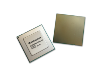
Broadcom ships its 25.6 Tbps Tomahawk 4 

Broadcom has begun commercial shipments of its 25.6 Tbps StrataXGS Tomahawk 4 Ethernet switching silicon -- representing double the bandwidth of any other switch silicon currently on the market. The 25.6 Tbps capacity enables port densities of up to 64 × 400GbE, 128 × 200GbE, 256 × 100GbE, 256 × 40GbE, 256 × 25GbE, or 256 × 10GbE ports. Tomahawk 4, which is implemented in 7nm technology with 512 50G PAM4 SerDes, arrives less than two years after...

Broadcom delivers its 12.8 Tbps Tomahawk 3 switching silicon

Broadcom announced commercial shipments of its StrataXGS Tomahawk 3 Ethernet switch silicon boasting 12.8 Terabits/sec in a single device -- double that of any other switching chip currently in the market. Tomahawk 3 paves the way for high-density, standards-based 400GbE, 200GbE, and 100GbE switching and routing for hyperscale cloud networks. The latest gen silicon is expected to be adopted by leading network equipment OEMs as well as by hyperscale...


Broadcom's Tomahawk 2 Switch Packs 64 Ports of 100GE 

Broadcom announced its StrataXGS Tomahawk II Switching chip -- the highest performance Ethernet switch to date, packing up to 64 ports 100GE or 128 ports of 50GE with SDN-optimized packet switch engines operating at 6.4 Terabits per second. The StrataXGS Tomahawk II  Tomahawk II integrates 256 serdes running at over 25 Gbps, with large on-chip forwarding tables and packet buffer memory.  The chip supports Broadcom's next generation BroadView...