Showing posts with label Silicon Photonics. Show all posts

Sunday, September 18, 2022

ECOC22: Broadcom’s Silicon Photonics Chiplets in Package

What's Next at #ECOC22 for Broadcom? 

Broadcom's Silicon Photonics Chiplet in Package (SCIP). 

Rebecca Schaevitz, Product Line Manager & Principal Engineer at Broadcom, provides an introduction. 

Learn more about the Consortium for Onboard Optics and why your company should join:

https://www.onboardoptics.org

https://youtu.be/UWmcFN_y25w

Wednesday, August 10, 2022

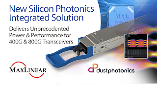
DustPhotonics and MaxLinear demo silicon photonics + integrated lasers

DustPhotonics and MaxLinear demonstrated a silicon photonics chipset with integrated lasers directly driven from a DSP without the use of any external driver chip.

The MaxLinear Keystone DSP (Digital Signal Processor) and DustPhotonics Carmel Silicon Photonics chip were shown together to support direct-drive operation, which reduces the overall cost and power dissipation of optical transceivers for data communication. 

Potential applications include 400 Gbps and 800 Gbps pluggable modules and on-board optics.

The DustPhotonics chip includes an integrated DFB (Distributed-feedback) laser and DustPhotonics Low Loss Laser Coupling technology (L3C), achieving a very efficient coupling of light into the Photonic Integrated Circuit (PIC). This unique technology enables the use of 1 laser for every 4 channels.

The MaxLinear Keystone chip is part of a family of DSPs capable of both 400 Gbps and 800 Gbps operation, based on TSMC’s 5nm process. The Keystone DSP provides a rich set of features for transceivers, CPO (Co-Packaged Optics) modules and on-board optics while achieving significantly lower power than competitive solutions. The integrated drivers are optimized for silicon photonics direct-drive and provide the best industry performance for this application.

The companies say their combined solution enables performance that significantly exceeds all IEEE specifications. In terms of power consumption, 400 Gbps transceivers can now be designed to reach sub 7W.

“DustPhotonics is focused on enabling best-in-class Silicon Photonics chips to simplify the efforts of transceiver and systems designers,” said Yoel Chetrit, Vice President R&D of DustPhotonics. “Not only can our Carmel chip simplify the overall system design by reducing the total number of lasers to a single laser for 4 channels, but it also eliminates the external driver, which reduces the cost, power and complexity of the overall system.”

“The combination of our Keystone 5nm integrated driver DSPs with DustPhotonics’ silicon photonics demonstrates the significant power and performance advantages achievable with our integrated drivers,” said Drew Guckenberger, Vice President of Optical Interconnect at MaxLinear. “With double-digit year-on-year growth in market demand for 400Gb/s and 800Gb/s transceivers, this integrated solution can create tremendous value for our customers. We look forward to seeing full transceiver deployments in the near future.”

http://www.dustphotonics.com

http://www.maxlinear.com


MaxLinear, MACOM and II-VI eye 800G modules

MaxLinear, MACOM and II-VI, demonstrated 100G/lane multi-mode links targeted for 800G optical modules. These links incorporate the MaxLinear Keystone 5nm 800G DSP, MACOM 100G/lane TIAs and VCSEL drivers and II-VI latest 850nm VCSELs and photodetectors.MaxLinear's Keystone family of 5nm PAM4 DSPs includes 400G and 800G variants with and without integrated laser drivers. This demonstration uses the 800G DSP, in conjunction with the MACOM four-channel...

MaxLinear showcases 5nm CMOS 800G PAM4 DSP

MaxLinear will showcase a 5nm CMOS 800Gbps PAM4 DSP for data center applications at the virtual Optical Fiber Communication Conference and Exhibition (OFC) from June 6 to June 11, 2021. “With the exponential growth of data traffic within hyperscale cloud networks, the needed increase in interconnect bandwidth in those networks requires lower-power, higher-density optical modules that support higher lane rates,” said Drew Guckenberger, Vice President...


Thursday, June 23, 2022

Scintil Photonics raises $14M for silicon photonic integrated circuits

Scintil Photonics, a supplier of advanced silicon photonic integrated circuits with monolithically integrated lasers and optical amplifiers, secured €13.5M ($14.4M) in second round funding. The company is based in Grenoble, France.

Robert Bosch Venture Capital (RBVC) led the round, with historic shareholders Innovacom, Supernova Invest and Bpifrance, through its Digital Venture fund, reinvesting to bring the company’s total funding to €17.5M ($18.8M), to date.'

Scintil Photonics will use the funds to take its industrialization program to the next level and speed up the global commercialization of its products that boost communications in data centers, High-Performance Computing (HPC) and 5G networks. 

Scintil Photonics’ optical communications aim to significantly enhance traditional high-speed system and chip interconnections. The company’s Augmented Silicon Photonic Integrated Circuit (IC) product is a single-chip solution consisting of active and passive components, all made entirely from standard silicon photonics processes available at CMOS commercial foundries, and where III-V optical amplifiers and lasers are integrated on the backside of advanced silicon photonic circuits. This unique all-in-one integration of amplifiers and lasers enables ultrahigh-speed communications, due to extensive parallelization and higher bit rates, e.g., from 800 G to 3,200 Gbit/sec with very compact chips. 

“Scintil Photonics’ monolithic integration of III-V Lasers into silicon photonic chips is a key enabler for next-generation telecom, datacom and sensing,” says Ingo Ramesohl, managing director at RBVC. “The CMOS-compatible process allows for higher design freedom, lower losses and a smaller footprint at low cost. We are excited to partner with Scintil Photonics as it uniquely unlocks further miniaturization and integration of Photonic Integrated Circuits.” 


Scintil Photonics raises EUR 4 million for 800G transceiver prototype

Scintil Photonics, a start-up based in Grenoble, France, announced EUR 4 million in first-round funding for its work in silicon photonic fully integrated circuits. The company said the funding will be used to develop prototypes (800 Gbps transceiver photonic circuits) in commercial semiconductor foundries in order to sample strategic customers in the data center market. The team and development partnerships, including those with CEA-Leti in France...

Continuous-Wave Wavelength Division Multiplexing MSA gets underway

A new Continuous-Wave Wavelength Division Multiplexing Multi-Source Agreement (CW-WDM MSA) consortium has been established to define and promote specifications for multi-wavelength advanced integrated optics. The CW-WDM MSA said it will solely focus on specifying the laser source instead of the full communications link, and is not targeted at any specific application. Such an approach allows developers to fully optimize optics to their customers’...


Monday, April 4, 2022

Synopsys and Juniper form joint venture for silicon photonics

Synopsys and Juniper Networks are establishing a joint venture company focused on open silicon photonics for applications such as telecom, datacom, LiDAR, healthcare, HPC, AI, and optical computing. 

The new company's open silicon photonics platform will include integrated lasers, optical amplifiers, and a full suite of photonic components to form a complete solution that will be accessible through a Process Design Kit (PDK). The platform promises the lowest power consumption for high-performance Photonic Integrated Circuits (PICs). 

The new company, which has not yet been named, will be jointly owned, with Synopsys holding the majority share. It is being formed, in part, from the carve-out of integrated silicon photonics assets from Juniper, which includes more than 200 patents on photonic device design and process integration.

While part of Juniper, the new company has closely collaborated with Tower Semiconductor to develop and qualify Tower Semiconductor's PH18DA process technology to enable the industry's first "laser-on-a-chip" open silicon photonics platform. To demonstrate capabilities of this platform and accelerate customer adoption of the technology, the new company has created 400G and 800G photonics reference designs with integrated lasers and expects first samples to be available in summer 2022.

A key challenge for silicon photonics has been the cost of adding discrete lasers, which includes the manufacturing as well as the assembly and alignment of those lasers onto the photonic chip. This becomes more important as the number of laser channels and the overall bandwidth increases. By processing the Indium Phosphide (InP) materials directly onto the silicon photonics wafer, the PH18DA platform reduces the cost and time of adding lasers, enabling volume scalability and improved power efficiency. In addition, monolithically integrated lasers on silicon wafers improves overall reliability and simplifies packaging. This "Laser-on-a-Chip" open silicon photonics platform will bring integrated photonics to a host of new applications and markets that were previously not thought possible. The first Multi-Project Wafer (MPW) is scheduled to be taped out in Q2 2022.

"Silicon photonics is a rapidly growing market that is transforming many industries and creating exciting opportunities for new applications in the future," said Sassine Ghazi, president and chief operating officer at Synopsys. "The new company's open silicon photonics platform, combined with Synopsys' existing investment in a unified electronic photonic design automation solution consisting of OptoCompiler™, OptSim™, PrimeSim™, Photonic Device Compiler and IC Validator™ products, will help reshape the optical computing industry, enabling companies to cost-effectively shift to integrated lasers and significantly accelerate development of photonic IC designs."

"This revolutionary technology will change the economics of how people are going to build photonic systems," said Rami Rahim, CEO of Juniper Networks. "We have been strong supporters of integrated silicon photonics and we believe the new company will drive development of these systems by using an advanced open platform that will dramatically reduce costs and increase the performance and reliability of designs across multiple use cases. We are excited to continue to collaborate with the new company to enable a broad ecosystem to efficiently develop next-generation optical transceiver and co-packaged designs."

"We have had a long history of successful collaboration with Juniper Networks on integrated photonics. The new company formed by Synopsys and Juniper will strengthen and accelerate the adoption of the silicon photonics platform," said Russell Ellwanger, CEO of Tower Semiconductor. "Providing an open silicon photonics platform consisting of integrated lasers that has been qualified on Tower's process will enable customers to create innovative products with the potential to transform the industry."

https://www.synopsys.com

Juniper picks Synopsys for developing photonics-enabled chips

Synopsys is supplying its OptoCompiler platform, including the OptSim and PrimeSim HSPICE simulation solutions, to Juniper Networks to accelerate the development of photonic-enabled chips for the next generation of optical communications.Juniper plans to use Synopsys solutions to design and optimize its hybrid silicon and InP optical platform."Synopsys offers a unique, unified photonic and electronic design suite, which accelerates customer design...

Tower Semi and Juniper develop silicon photonics process 

Tower Semiconductor and Juniper Networks announced a silicon photonics (SiPho) foundry-ready process with integrated III-V lasers, amplifiers modulators and detectors. 

Potential applications include optical connectivity in datacenters and telecom networks, as well as AI, LiDAR and other sensors. 

The new platform co-integrates III-V lasers, semiconductor optical amplifiers (SOA), electro-absorption modulators (EAM) and photodetectors with silicon photonics devices, all monolithically on a single chip. This enables smaller, higher-channel count and more power-efficient optical architectures and solutions. Foundry availability will enable a broad array of product developers to create highly integrated photonic integrated circuits (PICs) for diverse markets.   

Process design kits (PDK) are expected to be available by year end and the first open multi-project wafer (MPW) run are expected to be offered early next year. First samples of full 400Gb/s and 800Gb/s PICs reference designs with integrated laser are expected to be available in the second quarter of 2022. 

“Our mutual development work with Tower has been extraordinarily successful in qualifying this innovative silicon photonics technology in a high-volume manufacturing facility,” said Rami Rahim, CEO of Juniper Networks. “By offering this capability to the entire industry, Juniper offers the potential to radically reduce the cost of optics while lowering the barrier to entry for customers”. 

“Our partnership with Juniper on silicon photonics is bringing a paradigm shift for product development across our industry,” said Russell Ellwanger, CEO of Tower Semiconductor. “It is now possible to mix the advantages of III-V semiconductors with high-volume silicon photonics manufacturing. Being the singular open market, integrated laser silicon photonics platform, and having a multi-year advantage over any potential foundry competitor, we are jointly creating breakthrough products with truly unique value for our industry and for society as a whole”. 

https://towersemi.com/2021/12/21/12212021/

Tuesday, March 1, 2022

EVG and Teramount target wafer-level silicon photonics packaging

EV Group (EVG), a leading supplier of wafer bonding and lithography equipment for the MEMS, nanotechnology and semiconductor markets, announced a collaboration with Teramount on implementing wafer-level optics.

The collaboration will leverage EVG's nanoimprint lithography (NIL) technology, expertise and services with Teramount's PhotonicPlug technology.

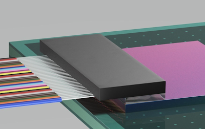
Under this collaboration, standard CMOS wafers that implement silicon photonics chips will be post processed using EVG's NIL technology to implement optical elements such as mirrors and lenses for Teramount's unique "self-aligning optics". This enables flexible beam extraction from the chips and easy connection to a large number of optical fibers. Furthermore, it enables wafer-level optical inspection capabilities for enhancing silicon photonics wafer manufacturing.

The collaboration is being carried out within EVG's NILPhotonics Competence Center at its headquarters in St. Florian, Austria. The NILPhotonics Competence Center provides an open access innovation incubator for customers and partners across the NIL supply chain to collaborate to shorten development cycles and time to market for innovative photonic devices and applications. Through the collaboration with Teramount, EVG provides process development and production services, as well as expertise in both CMOS and photonics manufacturing, thus accelerating the commercialization of Teramount's PhotonicPlug technology.

"Our joint work with EVG has been very successful in producing this innovative synergy between wafer-level optics and silicon photonics wafer manufacturing," said Hesham Taha, CEO of Teramount. "By offering this capability to the industry, Teramount solves one of the major hurdles to further adoption of optical connectivity, which is critical for so many applications that require high-speed data transfers and low power consumption."

"Teramount's PhotonicPlug silicon photonics packaging technology is a truly novel approach to improving optical performance, and we are excited to be a partner in helping to bring it to the market," stated Markus Wimplinger, Corporate Technology Development and IP Director at EV Group. "This is just the latest example of innovative technology developed with the support of EVG's process and equipment know-how through our NILPhotonics Competence Center, where we help our partners and customers turn new ideas into innovative products."

http://www.EVGroup.com

http://www.teramount.com

Tuesday, February 1, 2022

Aeva debuts 4D LiDAR on silicon photonics chip

Aeva, a start-up based in Mountain View, California, introduced a "4D LiDAR" sensor based on a unique Frequency Modulated Continuous Wave (FMCW) technology and a LiDAR-on-chip module design. The sensor uniquely detects the fourth dimension of instantaneous velocity for each point in addition to 3D position. 

Aeva’s LiDAR-on-Chip design eliminates all fiber optics and places all key components including transmitters, receivers and optics onto a silicon photonics chip in a compact module.

Aeva's 4D Perception software powers features like 4D Localization and Ultra Resolution, a camera-level image with up to 20 times the resolution of legacy LiDAR sensors. 

Key features :

  • Camera-Level Ultra Resolution: Leverages Aeva’s proprietary raw 4D data to deliver a real-time camera-level image with up to 1000 lines per frame with no motion blur for the static scene
  • Instant Velocity with Ultra Long Range: Aeva’s next-generation 4D LiDAR uniquely measures instantaneous velocity for each pixel in addition to 3D position, allowing automated vehicles and machines to perceive where things are and know precisely how fast they are moving, at distances up to 500 meters
  • LiDAR-on-Chip Technology: A groundbreaking design eliminates all fiber optics and incorporates all key LiDAR elements onto silicon photonics in a single compact module for reliable and scalable production
  • Automotive Grade Reliability: With automotive-grade ratings for ingress, impact, thermal, and shock and vibration to ensure peak performance across a variety of road and environmental conditions
  • Designed for Versatility: At a quarter of the size of the previous generation, the compact design allows for a wide range of integration options, with real-time configurable maximum ranges, field of views and scan patterns to enable a broad range of autonomous applications

“Aeries II is a leap forward for the industry, and we believe it will play a critical role in unlocking the next wave of automation across a variety of applications from automotive, to industrial and beyond,” said Mina Rezk, Co-Founder and CTO at Aeva. “Aeva's unique FMCW technology has inherent advantages like instant velocity detection for each point that allow us to deliver several crucial breakthroughs for our customers such as Ultra Resolution and 4D Localization, which have not been possible until today. Aeries II provides our customers with a new level of perception to help automated vehicles and machines make safer, more intelligent decisions with higher confidence.”

https://www.aeva.com/aeries-ii/

Thursday, December 23, 2021

Juniper picks Synopsys for developing photonics-enabled chips

Synopsys is supplying its OptoCompiler platform, including the OptSim and PrimeSim HSPICE simulation solutions, to Juniper Networks to accelerate the development of photonic-enabled chips for the next generation of optical communications.

Juniper plans to use Synopsys solutions to design and optimize its hybrid silicon and InP optical platform.

"Synopsys offers a unique, unified photonic and electronic design suite, which accelerates customer design cycles and time-to-market," said Tom Mader, head of Silicon Photonics at Juniper Networks. "This will enable Juniper silicon photonics to bring our revolutionary hybrid integrated laser platform to a broad array of customers in several photonic market segments, with the potential to lower cost and eliminate product barriers to entry."

Synopsys says its OptSim solution brings together photonic system and circuit simulation capabilities and provides electro-optical (E/O) co-simulation with the Synopsys PrimeSim HSPICE Simulator, the industry's 'gold standard' for accurate circuit simulation and the cornerstone of the Synopsys PrimeSim Continuum Solution. It also integrates seamlessly with the Synopsys PrimeWave design environment, the simulation and analysis environment of the OptoCompiler platform. The OptSim solution comes with an extensive photonic model library and is enabled for a wide variety of photonic IC foundries.

"Demand for higher bandwidth in intra-data center communications is driving companies like Juniper to deploy silicon photonic solutions to achieve the next level in performance," said Aveek Sarkar, VP of Customer Success for Analog Mixed-Signal/Custom & Photonics at Synopsys. "Synopsys is a pioneering solution provider in delivering robust solutions for electrical/optical co-design and co-simulation to enable next-generation photonic chips."

http://www.synopsys.com

Tuesday, December 21, 2021

Tower Semi and Juniper develop silicon photonics process

Tower Semiconductor and Juniper Networks announced a silicon photonics (SiPho) foundry-ready process with integrated III-V lasers, amplifiers modulators and detectors. 

Potential applications include optical connectivity in datacenters and telecom networks, as well as AI, LiDAR and other sensors. 

The new platform co-integrates III-V lasers, semiconductor optical amplifiers (SOA), electro-absorption modulators (EAM) and photodetectors with silicon photonics devices, all monolithically on a single chip. This enables smaller, higher-channel count and more power-efficient optical architectures and solutions. Foundry availability will enable a broad array of product developers to create highly integrated photonic integrated circuits (PICs) for diverse markets.   

Process design kits (PDK) are expected to be available by year end and the first open multi-project wafer (MPW) run are expected to be offered early next year. First samples of full 400Gb/s and 800Gb/s PICs reference designs with integrated laser are expected to be available in the second quarter of 2022. 

“Our mutual development work with Tower has been extraordinarily successful in qualifying this innovative silicon photonics technology in a high-volume manufacturing facility,” said Rami Rahim, CEO of Juniper Networks. “By offering this capability to the entire industry, Juniper offers the potential to radically reduce the cost of optics while lowering the barrier to entry for customers”. 

“Our partnership with Juniper on silicon photonics is bringing a paradigm shift for product development across our industry,” said Russell Ellwanger, CEO of Tower Semiconductor. “It is now possible to mix the advantages of III-V semiconductors with high-volume silicon photonics manufacturing. Being the singular open market, integrated laser silicon photonics platform, and having a multi-year advantage over any potential foundry competitor, we are jointly creating breakthrough products with truly unique value for our industry and for society as a whole”. 

https://towersemi.com/2021/12/21/12212021/

Wednesday, December 8, 2021

Intel establishes Integrated Photonics Research Center

Intel Labs has established an academically-oriented Integrated Photonics Research Center with a mission to accelerate optical input/output (I/O) technology innovation in performance scaling and integration with a specific focus on photonics technology and devices, CMOS circuits and link architecture, and package integration and fiber coupling.

The Intel Research Center for Integrated Photonics for Data Center Interconnects will bring together leading university researchers to accelerate optical I/O technology innovation in performance scaling and integration. The research vision is to explore a technology scaling path that satisfies energy efficiency and bandwidth performance requirements for the next decade and beyond. 

"At Intel Labs, we’re strong believers that no one organization can successfully turn all the requisite innovations into research reality. By collaborating with some of the top scientific minds from across the United States, Intel is opening the doors for the advancement of integrated photonics for the next generation of compute interconnect. We look forward to working closely with these researchers to explore how we can overcome impending performance barriers,” stated James Jaussi, senior principal engineer and director of the PHY Research Lab in Intel Labs.

The researchers participating in the Research Center include:

  • John Bowers, University of California, Santa Barbara
    Project: Heterogeneously Integrated Quantum Dot Lasers on Silicon.
    Description: The UCSB team will investigate issues with integrating indium arsenide (InAs) quantum dot lasers with conventional silicon photonics. The goal of this project is to characterize expected performance and design parameters of single frequency and multiwavelength sources.
  • Pavan Kumar Hanumolu, University of Illinois, Urbana-Champaign
    Project: Low-power optical transceivers enabled by duo-binary signaling and baud-rate clock recovery.
    Description: This project will develop ultra-low-power, high-sensitivity optical receivers using novel trans-impedance amplifiers and baud-rate clock and data recovery architectures. The prototype optical transceivers will be implemented in a 22 nm CMOS process to demonstrate very high jitter tolerance and excellent energy efficiency.
  • Arka Majumdar, University of Washington
    Project:
    Nonvolatile reconfigurable optical switching network for high-bandwidth data communication.
    Description: The UW team will work on low-loss, nonvolatile electrically reconfigurable silicon photonic switches using emerging chalcogenide phase change materials. Unlike existing tunable mechanisms, the developed switch will hold its state, allowing zero static power consumption.
  • Samuel Palermo, Texas A&M University
    Project:
    Sub-150fJ/b optical transceivers for data center interconnects.
    Description: This project will develop energy-efficient optical transceiver circuits for a massively parallel, high-density and high-capacity photonic interconnect system. The goal is to improve energy efficiency by employing dynamic voltage frequency scaling in the transceivers, low-swing voltage-mode drivers, ultra-sensitive optical receivers with tight photodetector integration, and low-power optical device tuning loops.
  • Alan Wang, Oregon State University
    Project:
    0.5V silicon microring modulators driven by high-mobility transparent conductive oxide.
    Description: This project seeks to develop a low driving voltage, high bandwidth silicon microring resonator modulator (MRM) through heterogeneous integration between the silicon MOS capacitor with high-mobility Ti:In2O3 The device promises to overcome the energy efficiency bottleneck of the optical transmitter and can be co-packaged in future optical I/O systems.
  • Ming Wu, University of California, Berkeley
    Project:
    Wafer-scale optical packaging of silicon photonics.
    Description: The UC Berkeley team will develop integrated waveguide lenses that have potential to enable non-contact optical packaging of fiber arrays with low loss and high tolerances.
  • S.J. Ben Yoo, University of California, Davis
    Project:
    Athermal and power-efficient scalable high-capacity silicon-photonic transceivers.
    Description: The UC Davis team will develop extremely power-efficient athermal silicon-photonic modulator and resonant photodetector photonic integrated circuits scaling to 40 Tb/s capacity at 150 fJ/b energy efficiency and 16 Tb/s/mm I/O density. To achieve this, the team will also develop a new 3D packaging technology for vertical integration of photonic and electronic integrated circuits with 10,000 pad-per-square-mm interconnect-pad-density.

https://www.intel.com/content/www/us/en/newsroom/news/intel-launches-integrated-photonics-research-center.html

Intel shows micro-ring modulators, all-silicon photodetectors, multi-lambda lasers

Intel showcased a number of advancements in the field of optical interconnects, advancing its long-term ambition to bring optical I/O directly into silicon packages. During a virtual Intel Labs day presentatio, the company demonstrated advances in key technology building blocks, including with light generation, amplification, detection, modulation, complementary metal-oxide semiconductor (CMOS) interface circuits and package integration. 

Key technology building blocks showcased:

  • Micro-ring modulators: Conventional silicon modulators take up too much area and are costly to place on IC packages. By developing micro-ring modulators, Intel has miniaturized the modulator by a factor of more than 1,000, thereby eliminating a key barrier to integrating silicon photonics onto a compute package.
  • All-silicon photodetector: For decades, the industry has believed silicon has virtually no light detection capability in the 1.3-1.6um wavelength range. Intel showcased research that proves otherwise. Lower cost is one of the main benefits of this breakthrough.
  • Integrated semiconductor optical amplifier: As the focus turns to reducing total power consumption, integrated semiconductor optical amplifiers are an indispensable technology, made possible with the same material used for the integrated laser.
  • Integrated multi-wavelength lasers: Using a technique called wavelength division multiplexing, separate wavelengths can be used from the same laser to convey more data in the same beam of light. This enables additional data to be transmitted over a single fiber, increasing bandwidth density.
  • Integration: By tightly integrating silicon photonics and CMOS silicon through advanced packaging techniques, we can gain three benefits: lower power, higher bandwidth and reduced pin count. Intel is the only company that has demonstrated integrated multi-wavelength lasers and semiconductor optical amplifiers, all-silicon photodetectors, and micro-ring modulators on a single technology platform tightly integrated with CMOS silicon. This research breakthrough paves the path for scaling integrated photonics.

Intel said these advancements will enable future architectures that are more disaggregated, with multiple functional blocks such as compute, memory, accelerators and peripherals spread throughout the entire network and interconnected via optical and software in high-speed and low-latency links.

“We are approaching an I/O power wall and an I/O bandwidth gap that will dramatically hinder performance scaling. The rapid progress Intel is making in integrated photonics will enable the industry to fully re-imagine data center networks and architectures that are connected by light. We have now demonstrated all of the critical optical technology building blocks on one silicon platform, tightly integrated with CMOS silicon. Our research on tightly integrating photonics with CMOS silicon can systematically eliminate barriers across cost, power and size constraints to bring the transformative power of optical interconnects to server packages,” stated James Jaussi, senior principal engineer and director of PHY Lab, Intel Labs.

Without such advancements, Intel warns the industry will soon reach the practical limits of electrical I/O performance - what it calls an "I/O power wall".


https://www.intel.com/content/www/us/en/newsroom/news/progress-integrated-photonics-data-centers.html#gs.ibzo2u

Thursday, October 28, 2021

DustPhotonics raises $33M for its silicon photonics

DustPhotonics, a start-up based in Modi'in, Israel, announced $33 million in venture funding for its silicon photonics solutions for cloud, data center, enterprise and HPC applications. The company's InP Laser to Silicon Photonics integration technology will provide significant value differentiation enabling superior performance to support 800 Gbps, 1.6Tbps, CPO and future products.

The funding round was led by Greenfield Partners, who join DustPhotonics' Round B investors Intel Capital, veteran entrepreneur Avigdor Willenz, and others.

In addition, the company also announced it has completed an organizational realignment to support its strategic and business direction. The company will focus its resources on silicon photonics solutions and phase out its transceivers product line. 

As part of the reorganization, Ronnen Lovinger, president of DustPhotonics, has assumed the role of CEO. Ben Rubovitch, the company's previous CEO, has stepped down and will lead the business side of the company.

"This latest investment and the organizational changes will enable us to take advantage of new business opportunities and to continue focusing on serving our customers' strategic requirements. Our disruptive silicon photonics technology addresses their key and most challenging problems, creating scalable, cost-effective silicon photonics and driving it as the mainstream solution for the Cloud and Telecom markets," said Ronnen Lovinger, CEO of DustPhotonics. "We are thrilled at the continued confidence of our investors in our strategic direction."

"With the rapid evolution of the connectivity and silicon optics markets, there is a growing need for innovative technologies. DustPhotonics is well-positioned at the forefront of silicon photonics technology development and we are excited to take part in their journey," said Yuda Doron, Managing Partner at Greenfield Partners.

http://www.dustphotonics.com 


Sunday, October 24, 2021

Anello raises $28M for silicon photonic optical gyroscope

Anello Photonics, a start-up based in Santa Clara, California, announced $28 million in Series A funding for its Silicon Photonic Optical Gyroscope (SiPhOG) sensor technology.

Anello says its novel SiPhOG replaces the discrete optical components of a traditional Fiber Optic Gyroscope (FOG) and combines high precision with greatly reduced size, weight, power and cost. The technology combines an Anello-developed on-chip waveguide manufacturing process integrated with a patented silicon photonic chip-scale gyroscope. 

Applications for the SiPhOG sensor technology could include automotive, trucking, construction, drone, aerospace, defense and consumer electronics.   

The Series A funding was led by New Legacy Ventures and included investments from Lockheed Martin Ventures, Catapult Ventures, JS Capital, Hardware Club, and individual investments from several Silicon Valley luminaries.

"With the development of the SiPhOG we are going to change the Navigation industry," says Mario Paniccia, Chief Executive Officer and co-founder of Anello. "We are bringing all the benefits of optical gyro performance onto an integrated silicon photonic circuit platform."

"By providing an independent and accurate ground truth of vehicle position, Anello's sensor and IMU system improves the reliability of Autonomous Vehicle localization while reducing the vulnerability to cyber-security threats and environmental interference common to other localization sensors," says Mike Horton, Chief Strategy Officer and co-founder of Anello.

http://www.anellophotonics.com

Wednesday, September 15, 2021

GlobalFoundries announces 45nm Silicon Photonics platform

GlobalFoundries announced a  new Silicon Photonics 45nm platform for combining RF CMOS and optical components on the same chip.

The monolithic platform includes an innovative new feature, the first micro ring resonator (MRR) optical component in 300 mm wafer technology.

GF said the new platform has passed critical technology milestones and is on track for full technology qualification by Q1 2022. The company also confirms that it is engaged with leading customers and partners on this new platform.


https://gf.com/blog/gf-innovation-moving-data-light-speed

Ayar Labs demos terabit link for Co-Packaged Optics and chip-to-chip

Ayar Labs demonstrated the industry’s first Terabit per second Wavelength Division Multiplexing (WDM) optical link with its TeraPHY optical I/O chiplet and SuperNova multi-wavelength optical source. The demonstration shows a fully functional TeraPHY chiplet with 8 optical ports running error free without Forward Error Correction (FEC) for a total bandwidth of 1.024 Tbps and at less than 5 pJ/bit energy efficiency. “This is yet another industry...

GlobalFoundries adapts silicon photonics for quantum computing

GlobalFoundries is now manufacturing the silicon photonic and electronic chips that form the foundation of PsiQuantum's Q1 quantum computer.

PsiQuantum, a start-up based in Palo Alto, California, aims to be the first to deliver a commercially viable quantum computer with one million qubits.

PsiQuantum and GF have now demonstrated the ability to manufacture core quantum components, such as single-photon sources and single-photon detectors, with precision and in volume, using the standard manufacturing processes of GF’s semiconductor fab. The companies have also installed proprietary production and manufacturing equipment in two of GF’s 300mm fabs to produce thousands of Q1 silicon photonic chips at its facility in upstate New York, and state-of-the-art electronic control chips at its Fab 1 facility in Dresden, Germany.

PsiQuantum’s Q1 system represents breakthroughs in silicon photonics, which the company believes is the only way to scale to 1 million-plus qubits and beyond and to deliver an error-corrected, fault-tolerant, general-purpose quantum computer.

“In the past year, we have experienced a decade of technological change. Now, due to the digital transformation and the explosion of data we are faced with problems that require quantum computing to further accelerate the Renaissance of Compute,” said Amir Faintuch, senior vice president and general manager of Compute and Wired Infrastructure at GF. “PsiQuantum and GF’s partnership is a powerful combination of PsiQuantum’s photonic quantum computing expertise and GF’s silicon photonics manufacturing capability that will transform industries and technology applications across climate, energy, healthcare, materials science, and government.”

“This is a major achievement for both the quantum and semiconductor industries, demonstrating that it’s possible to build the critical components of a quantum computer on a silicon chip, using the standard manufacturing processes of a world-leading semiconductor fab,” said Pete Shadbolt, chief strategy officer and co-founder of PsiQuantum. “When we first envisioned PsiQuantum, we knew that scaling the system would be the existential question. Together with GLOBALFOUNDRIES, we have validated the manufacturing path for silicon photonics and are confident that by the middle of this decade, PsiQuantum will have completely stood up all the manufacturing lines and processes necessary to begin assembling a final machine.”

Tuesday, September 7, 2021

Keysight unveils Silicon Photonics Test System

 Keysight Technologies introduced a silicon photonics test system that enables semiconductor manufacturers to speed delivery of silicon photonics wafer production with stable and repeatable test capabilities.

The new NX5402A Silicon Photonics Test System integrated with Keysight PathWave Semiconductor Test software technology (part of Keysight PathWave Test software) delivers:

  • One-stop: Provides proven measurement technologies and direct support capabilities including integrated optical and electrical test capabilities and Keysight-developed fiber alignment and positioning system based on Keysight’s measurement science.
  • Fully automated: Eliminates manual operations with PathWave Semiconductor Test software which is compatible with Keysight’s SPECS software, enabling one-pass silicon photonics testing.
  • Volume production ready: Factory automation software, safety interlock and clean room ready features support manufacturing use, providing high throughput testing based on multi-channel optical and electrical test architecture, as well as optimized fiber alignment.
  • Demonstrated system performance: Maintains high accuracy, repeatability and reproducibility from laboratory to fabrication, delivering advanced wafer-level photonic calibration, as well as reliable performance monitoring with built-in automatic system diagnostics.

"Ahead of the growing market demand for silicon photonics, Keysight is excited to announce the first test solution for silicon photonics volume production market,” said Shinji Terasawa, vice president and general manager of Keysight’s Wafer Test Solutions group. “Our NX5402A test system is the first solution that combines Keysight’s expertise in electrical and optical measurement with Keysight’s fiber alignment and positioning system integrated by PathWave Semiconductor Test software."

http://www.keysight.com

Sunday, June 13, 2021

Silicon Photonics integration of Indium phosphide distributed feedback lasers

Sivers Photonics, imec, and ASM AMICRA successfully completed a wafer-scale integration of indium phosphide (InP) distributed feedback (DFB) lasers from Sivers’ InP100 platform onto imec’s silicon photonics platform (iSiPP). 

Using ASM AMICRA’s latest NANO flip-chip bonder tool, the InP DFB laser diodes were bonded onto a 300mm silicon photonics wafer with an alignment precision within 500nm, enabling reproducible coupling of more than 10mW of laser power into the silicon nitride waveguides on the silicon photonics wafer. Supported by its partners, imec will offer this technology later in 2021 as a prototyping service, thereby accelerating the adoption of silicon photonics in a wide range of applications from optical interconnects, over LiDAR, to biomedical sensing.

Sivers says many silicon photonic systems today still rely on external light sources, owing to the lack of efficient on‐chip light sources. Silicon itself does not emit light efficiently and, therefore, light sources made of III-V semiconductors, such as indium phosphide (InP) or gallium arsenide (GaAs), are typically implemented as separately packaged components. These off‐chip lasers often suffer from higher coupling losses, a large physical footprint and a high packaging cost.

“We’re excited to work with imec and ASM AMICRA on the development of advanced integrated photonic components. The availability of tailored InP laser sources, designed and fabricated on our InP100 manufacturing platform, will boost the adoption of silicon photonic circuits for a wide variety of commercial applications ”, says Billy McLaughlin, Sivers Photonics Managing Director.

Joris van Campenhout, Optical I/O Program Director at imec: “We are very pleased to be working with Sivers Photonics and ASM AMICRA to extend our silicon photonics platform with hybrid integrated laser sources and amplifiers. This additional functionality will enable our joint customers to develop and prototype advanced photonic integrated circuits (PICs) with capabilities well beyond what we can offer today, in key areas such as datacom, telecom and sensing.”

Dr. Johann Weinhändler, ASM AMICRA Managing Director: “Our strength in high-precision placement seamlessly complements the expertise of all partners. With automated and ultra-precise flip-chip bonding, the way to high-volume manufacturing of these hybrid assemblies is open.”

Wednesday, May 5, 2021

GlobalFoundries adapts silicon photonics for quantum computing

GlobalFoundries is now manufacturing the silicon photonic and electronic chips that form the foundation of PsiQuantum's Q1 quantum computer.

PsiQuantum, a start-up based in Palo Alto, California, aims to be the first to deliver a commercially viable quantum computer with one million qubits.

PsiQuantum and GF have now demonstrated the ability to manufacture core quantum components, such as single-photon sources and single-photon detectors, with precision and in volume, using the standard manufacturing processes of GF’s semiconductor fab. The companies have also installed proprietary production and manufacturing equipment in two of GF’s 300mm fabs to produce thousands of Q1 silicon photonic chips at its facility in upstate New York, and state-of-the-art electronic control chips at its Fab 1 facility in Dresden, Germany.

PsiQuantum’s Q1 system represents breakthroughs in silicon photonics, which the company believes is the only way to scale to 1 million-plus qubits and beyond and to deliver an error-corrected, fault-tolerant, general-purpose quantum computer.

“In the past year, we have experienced a decade of technological change. Now, due to the digital transformation and the explosion of data we are faced with problems that require quantum computing to further accelerate the Renaissance of Compute,” said Amir Faintuch, senior vice president and general manager of Compute and Wired Infrastructure at GF. “PsiQuantum and GF’s partnership is a powerful combination of PsiQuantum’s photonic quantum computing expertise and GF’s silicon photonics manufacturing capability that will transform industries and technology applications across climate, energy, healthcare, materials science, and government.”

“This is a major achievement for both the quantum and semiconductor industries, demonstrating that it’s possible to build the critical components of a quantum computer on a silicon chip, using the standard manufacturing processes of a world-leading semiconductor fab,” said Pete Shadbolt, chief strategy officer and co-founder of PsiQuantum. “When we first envisioned PsiQuantum, we knew that scaling the system would be the existential question. Together with GLOBALFOUNDRIES, we have validated the manufacturing path for silicon photonics and are confident that by the middle of this decade, PsiQuantum will have completely stood up all the manufacturing lines and processes necessary to begin assembling a final machine.”