Showing posts with label Samsung. Show all posts

Monday, December 5, 2022

Samsung and NAVER target semiconductors for hyperscale AI

Samsung Electronics and NAVER Corporation are collaborating on semiconductor solutions tailored for hyperscale artificial intelligence (AI) models. 

The partnership leverages Samsung’s next-generation memory technologies like computational storage, processing-in-memory (PIM) and processing-near-memory (PNM), as well as Compute Express Link (CXL).

NAVER will continue to refine HyperCLOVA, a hyperscale language model with over 200 billion parameters, while improving its compression algorithms to create a more simplified model that significantly increases computation efficiency.

“Through our collaboration with NAVER, we will develop cutting-edge semiconductor solutions to solve the memory bottleneck in large-scale AI systems,” said Jinman Han, Executive Vice President of Memory Global Sales & Marketing at Samsung Electronics. “With tailored solutions that reflect the most pressing needs of AI service providers and users, we are committed to broadening our market-leading memory lineup including computational storage, PIM and more, to fully accommodate the ever-increasing scale of data.”

“Combining our acquired knowledge and know-how from HyperCLOVA with Samsung’s semiconductor manufacturing prowess, we believe we can create an entirely new class of solutions that can better tackle the challenges of today’s AI technologies,” said Suk Geun Chung, Head of NAVER CLOVA CIC. “We look forward to broadening our AI capabilities and bolstering our edge in AI competitiveness through this strategic partnership.”


Wednesday, November 30, 2022

Samsung to provide O-RAN radios for NTT DOCOMO


Samsung will provide Open RAN-compliant radios covering all of the TDD spectrum bands held by NTT DOCOMO — including 3.4GHz, 3.7GHz, 4.5GHz and 28GHz. The companies have tested the interoperability of these new radios with basebands from various vendors in NTT DOCOMO’s commercial network environment.

The announcement expands upong a 5G agreement previously announced in March 2021 in which NTT DOCOMO selected Samsung as its 5G network solutions provider

Samsung also introduced a new 28GHz Radio Unit (RU) for the first time — as a new addition to its portfolio of mmWave solutions. Weighing less than 10 lbs., the RU features a light and compact form factor with very low power consumption, enabling flexible deployments in various scenarios. NTT DOCOMO will use this new radio as part of their deployment.

“We have been collaborating with Samsung since the beginning of 5G and through our Open RAN expansion, and we are excited to continue extending our scope of vision together,” said Masafumi Masuda, Vice President and General Manager of the Radio Access Network Development Department at NTT DOCOMO. “Solidifying our global leadership, we will continue to build momentum around our Open RAN innovation and to provide highly scalable and flexible networks to respond quickly to the evolving demands of our customers.”

“Japan is home to one of the world’s most densely populated areas with numerous skyscrapers and complex infrastructure. Samsung’s industry-leading 5G radios portfolio meets the demands of low-footprint, low-weight solutions, while also ensuring reliable service quality,” said Satoshi Iwao, Vice President and Head of Network Division at Samsung Electronics Japan. 

https://news.samsung.com/us/samsung-expands-5g-radio-support-ntt-docomo/

KT, NTT DOCOMO and Fujitsu test O-RAN in Korea

The KT Research and Development Center in Seoul, South Korea, has tested Fujitsu’s Open RAN based 5G base station equipment in trials for open fronthaul. NTT DOCOMO provided Fujitsu with technical support throughout the project. With the construction of this new test facility, KT will accelerate the introduction of Open RAN technology to Korea’s 5G network.The three companies have concluded a Memorandum of Understanding centered on the introduction...


Monday, November 7, 2022

Samsung ships 8th gen Vertical NAND for enterprise servers

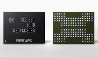
Samsung Electronics has begun mass producing a 1-terabit (Tb) triple-level cell (TLC) eighth-generation Vertical NAND (V-NAND) targeted at next-gen enterprise servers and automotive applications.

The new V-NAND boasts the industry’s highest bit density and also features the highest storage capacity (1 Tb) to date, enabling larger storage space in next-generation enterprise server systems worldwide.

Samsung was able to attain the industry’s highest bit density by significantly enhancing the bit productivity per wafer. Based on the Toggle DDR 5.0 interface, Samsung’s eighth-generation V-NAND features an input and output (I/O) speed of up to 2.4 Gbps, a 1.2X boost over the previous generation. This will enable the new V-NAND to accommodate the performance requirements of PCIe 4.0, and later, PCIe 5.0.

"As market demand for denser, greater-capacity storage pushes for higher V-NAND layer counts, Samsung has adopted its advanced 3D scaling technology to reduce surface area and height, while avoiding the cell-to-cell interference that normally occurs with scaling down," said SungHoi Hur, Executive Vice President of Flash Product & Technology at Samsung Electronics. "Our eighth-generation V-NAND will help meet rapidly growing market demand and better position us to deliver more differentiated products and solutions, which will be at the very foundation of future storage innovations."


Monday, October 17, 2022

Samsung's latest LPDDR DRAM clocks in at 8.5 Gbps

Samsung Electronics introduced its latest and fastest LPDDR DRAM to date: LPDDR5X DRAM boasts the industry’s fastest speed of 8.5 Gbps as validated for use on Snapdragon mobile platforms. 

By optimizing a high-speed signal environment between application processor and memory, Samsung has surpassed the previous maximum speed of 7.5Gbps achieved in March, reaffirming its leadership in the memory market.

For data centers and edge servers, LPDDR DRAM’s low-power characteristics can help reduce power consumption levels, resulting in an improved total cost of ownership (TCO) for data center managers, while cutting down on heat and carbon emissions to ultimately lower their impact on climate change.

“The joint validation of 8.5Gbps LPDDR5X DRAM has enabled us to accelerate market-wide availability of this high-speed memory interface by more than a year, which is a tremendous accomplishment made possible through our long-standing collaboration with Qualcomm Technologies,” said Daniel Lee, Executive Vice President of the Memory Product Planning Team at Samsung Electronics. “As LPDDR memory continues to broaden its usage beyond smartphones into AI and data center applications, strong collaboration between memory and SoC vendors is becoming all the more important. Samsung will continue to actively engage with innovators like Qualcomm Technologies to enhance ecosystem readiness for future LPDDR standards.”

“At Qualcomm Technologies, we strive to be at the forefront of enabling and adopting the latest memory specifications on our Snapdragon mobile platforms. We’re the first in the mobile industry to enable the latest LPDDR5X at 8.5Gbps on Snapdragon mobile platforms, which will enhance user experiences with new features and improved performance for mobile, gaming, camera and AI applications,” said Ziad Asghar, Vice President of Product Management, Qualcomm Technologies, Inc.

Monday, October 3, 2022

Samsung updates roadmap, aims for 1.4nm nodes in 2027

At its annual Samsung Foundry Forum event in San Jose, California, Samsung Electronics outlined its goals to drive process nodes to 1.4nm in 2027. 

Samsung, which currently has 3nm process technology in mass production, Samsung will be further enhancing gate-all-around (GAA) based technology and plans to introduce the 2nm process in 2025 and 1.4nm process in 2027.

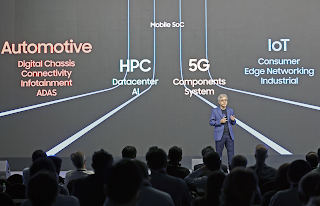
The event focused on foundry process technology innovation, process technology optimization for each specific applications, stable production capabilities, and customized services, including the enhancement its GAA-based 3nm process support for HPC and mobile applications. Samsung will also diversify the 4nm process for HPC and automotive applications.

For automotive customers specifically, Samsung is currently providing embedded non-volatile memory (eNVM) solutions based on 28nm technology. In order to support automotive-grade reliability, the company plans to further expand process nodes by launching 14nm eNVM solutions in 2024 and adding 8nm eNVM in the future. Samsung has been mass producing 8nm RF following 14nm RF, and 5nm RF is currently in development.

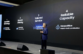
“The technology development goal down to 1.4nm and foundry platforms specialized for each application, together with stable supply through consistent investment are all part of Samsung’s strategies to secure customers’ trust and support their success,” said Dr. Si-young Choi, president and head of Foundry Business at Samsung Electronics. “Realizing every customer's innovations with our partners has been at the core of our foundry service."

Samsung also confirmed that its 3D packaging X-Cube with micro-bump interconnection will be ready for mass production in 2024, and bump-less X-Cube will be available in 2026.

In addition, Samsung highlighted its production expansion. The company plans to expand its production capacity for the advanced nodes by more than three times by 2027 compared to this year. Including the new fab under construction in Taylor, Texas, Samsung's foundry manufacturing lines are currently in five locations: Giheung, Hwaseong, and Pyeongtaek in Korea; and Austin and Taylor in the United States.

Wednesday, September 21, 2022

Comcast looks to Samsung for 5G RAN

Comcast is working with Samsung to deliver 5G Radio Access Network (RAN) solutions tfor Xfinity Mobile and Comcast Business Mobile customers in Comcast service areas. 

Specifically, Samsung will supply 5G RAN solutions to deliver 5G access to consumer and business customers in the United States using Citizens Broadband Radio Service (CBRS) and 600MHz spectrum.

Samsung 5G RAN products to be provided include radios for CBRS and 600MHz, baseband units, and a newly developed 5G CBRS Strand Small Cell that can be deployed on Comcast’s aerial cable lines (i.e. strand). Using the new compact and lightweight small cell product, Comcast can leverage its existing DOCSIS infrastructure without having to build or acquire additional cell sites.

“Our capital-light approach to providing enhanced 5G connectivity in service areas where we have a high concentration of traffic and cable infrastructure is smart for our business and even better for customers who will benefit from broader coverage and industry-leading speeds and prices,” said Tom Nagel, SVP of Wireless Strategy at Comcast. “Partnering with Samsung and leveraging their leadership in 5G network innovation will help us seamlessly deliver more next-generation applications and services to our consumer and business mobile customers.”

“We are excited to collaborate with Comcast on their journey to deliver the most enhanced 5G experiences available to their customers,” said Mark Louison, Executive Vice President and Head of Networks Business, Samsung Electronics America. “With this partnership, Samsung continues to build on its wireless technology leadership in commercial 5G rollouts. We look forward to helping Comcast advance its goals in delivering best-in-class 5G mobile services for their Xfinity Mobile and Comcast Business customers.”


Tuesday, August 9, 2022

Kajeet and Samsung collaborate on Private 5G

Kajeet, which specializes in private wireless and managed IoT connectivity solutions, will become an authorized distributor of Samsung’s private RAN solutions in the U.S.

The collaboration matches Kajeet’s Smart Private 5G Platform with Samsung’s Citizens Broadband Radio Service (CBRS) solutions. 

Samsung’s CBRS products to be deployed by Kajeet include its Massive MIMO 64T64R macro cell and 4T4R 4G/5G radio. Certified by the OnGo® Alliance, these products support a variety of use cases requiring campus-wide connectivity with massive data capacity. This includes enabling FWA for underserved rural areas and industrial IoT applications connecting thousands of sensors to analyze data.

Kajeet builds and manages private 5G networks on behalf of school districts, smart cities, municipalities, universities and community colleges, utilities, libraries, healthcare organizations, and other enterprises in key vertical markets.

"Samsung has been a pioneer in RAN innovation, and we are excited to be collaborating with them to address the needs of our expanding array of customers that want robust, reliable and affordable carrier-class private wireless networks,” said Derrick Frost, SVP and GM of Private Wireless Networks at Kajeet. “Kajeet’s open innovation in 5G edge & core, paired with Samsung’s CBRS solutions that enable seamless migration to 5G and suit any vertical use case, provides enhanced connectivity experiences both today and tomorrow.”

“Samsung is committed to advancing private network innovation and putting this technology into action for various enterprises and organizations today,” said Imran Akbar, Vice President and Head of New Business Team, Networks Business, Samsung Electronics America. “Kajeet has extensive experience in deploying and managing end-to-end private and public networks, and we look forward to collaborating with them to accelerate deployment of Samsung’s industry leading private 5G solutions to help lead digital transformation for enterprises.”

Wednesday, August 3, 2022

Samsung develops Memory-semantic SSD based on CXL

 At this week's Flash Memory Summit 2022, Samsung announced its 'Memory-semantic SSD', which combines the benefits of storage and DRAM memory. Leveraging Compute Express Link (CXL) interconnect technology and a built-in DRAM cache, Memory-semantic SSDs can achieve up to a 20x improvement in both random read speed and latency when used in AI and ML applications. Samsung’s Memory-semantic SSDs will be optimized to read and write small-sized data chunks at dramatically faster speeds.

Samsung’s telemetry technology gathers human-readable metadata from key components inside customers’ SSDs such as NAND flash and DRAM as well as SSD controllers and firmware. Based on this broad set of telemetry information, data centers can detect and prevent any potential problems ahead of time, enabling a more reliable and efficient operation.

Additionally, Samsung confirmed that the first UFS 4.0 mobile storage is scheduled to enter mass production this month. The new UFS 4.0 will be a critical component in flagship smartphones that require large amounts of data processing for features like high-resolution images and graphics-heavy mobile games, and will later be used in mobility, VR and AR.

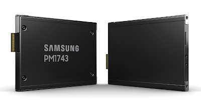
Samsung also announced market availability of two enterprise SSDs. Its PM1743 is the industry’s first PCIe 5.0 SSD, while the PM1653 is the first 24G SAS SSD, both now in mass production. The company further highlighted its paradigm-shifting SmartSSD and CXL DRAM, which have been designed to avoid bottlenecks in current memory and storage architectures.

"The IT industry is facing a new set of challenges brought on by the explosive growth in big data, and this underscores the importance of a robust, cross-industry ecosystem," said Jin-Hyeok Choi, keynote speaker and executive vice president of Memory Solution & Product Development at Samsung Electronics. "We are committed to developing transformative memory technologies that can bring far-reaching changes in how we move, store, process and manage data for future AI, ML and HPC applications, as we navigate these challenging tides together with industry partners."

Thursday, July 21, 2022

Samsung's 2nd gen SmartSSD computational drive offloads CPU

Samsung Electronics introduced a second generation of its pioneering SmartSSD computational storage drive that uses a Xilinx Versal Adaptive chip to offload certain data processing functionality from the host CPU.

Unlike existing SSDs, Samsung’s SmartSSD can process data directly, thereby minimizing data transfers between the CPU, GPU and RAM. This technology can avoid the bottlenecks that often occur when moving data between storage devices and CPUs, resulting in markedly improved system performance and much higher energy efficiency.

 Samsung says that compared to conventional data center solid-state drives, processing time for scan-heavy database queries can be slashed by over 50%, energy consumption by up to 70% and CPU utilization by up to 97%.

Since its development in 2020 through the joint efforts of Samsung and AMD, the first-generation SmartSSD is being supplied to global IT companies including video communications platform providers. The first-generation SmartSSD was recognized as an Innovation Awards Honoree at CES 2021 for its outstanding performance and energy efficiency.

 “Commercialization of the first-generation SmartSSD, in collaboration with AMD, established that the computational storage market has great potential,” said Jin-Hyeok Choi, Executive Vice President and Head of Memory Solution Product & Development at Samsung Electronics. “With the upgraded processing functionality of the second-generation SmartSSD, Samsung will be able to easily address increasing customer needs in the database and video transcoding sectors, as we expand the boundaries of the next-generation storage market.”

 “Powered by Xilinx Versal Adaptive SoCs from AMD, second-generation Samsung SmartSSDs enable improved CPU efficiency and greatly reduced energy consumption by efficiently integrating the computing and storage functions in data centers,” said Sina Soltani, Corporate Vice President of Sales, AECG, Data Center and Communication Group at AMD. “As data-intensive applications continue to grow, second-generation Samsung SmartSSDs will deliver the superior performance and efficiency required for this expanding market.”

 https://news.samsung.com/global/samsung-electronics-develops-second-generation-smartssd-computational-storage-drive-with-upgraded-processing-functionality

Wednesday, July 13, 2022

Samsung launches 24Gbps GDDR6 DRAM

Samsung Electronics has begun sampling the industry’s first 16-gigabit (Gb) Graphics Double Data Rate 6 (GDDR6) DRAM featuring 24 Gbps processing speeds. 

Built on Samsung’s third-generation 10-nanometer-class process using extreme ultraviolet (EUV) technology, the new memory is designed to significantly advance the graphics performance for next-generation graphics cards (Video Graphics Arrays), laptops and game consoles, as well as artificial intelligence-based applications and high-performance computing (HPC) systems.

Samsung claims its 24Gbps GDDR6 will deliver 30% faster speeds compared to the previous 18 Gbps product. When integrated into a premium graphics card, the GDDR6 DRAM can transfer up to 1.1-TB of data, or about 275 Full HD movies, in just one second.

"The explosion of data now being driven by AI and the metaverse is pushing the need for greater graphics capabilities that can process massive data sets simultaneously, at extremely high speeds," said Daniel Lee, executive vice president of the Memory Product Planning Team at Samsung Electronics. "With our industry-first 24Gbps GDDR6 now sampling, we look forward to validating the graphics DRAM on next-generation GPU platforms to bring it to market in time to meet an onslaught of new demand."

http://www.samsung.com

Wednesday, June 29, 2022

Samsung begins chip production using 3nm process

Samsung Electronics confirmed initial production of its 3-nanometer (nm) process node applying Gate-All-Around (GAA) transistor architecture. The company is starting the first application of the nanosheet transistor with semiconductor chips for high performance, low power computing applications and plans to expand to mobile processors.

Samsung says its proprietary technology utilizes nanosheets with wider channels, which allow higher performance and greater energy efficiency compared to GAA technologies using nanowires with narrower channels. Utilizing the 3nm GAA technology, Samsung will be able to adjust the channel width of the nanosheet in order to optimize power usage and performance to meet various customer needs.

"Samsung has grown rapidly as we continue to demonstrate leadership in applying next-generation technologies to manufacturing, such as the foundry industry’s first High-K Metal Gate, FinFET, as well as EUV. We seek to continue this leadership with the world’s first 3nm process with the MBCFET™," said Dr. Siyoung Choi, President and Head of Foundry Business at Samsung Electronics. "We will continue active innovation in competitive technology development and build processes that help expedite achieving maturity of technology.”

http://news.samsung.com

Tuesday, May 24, 2022

Samsung and Red Hat collaborate on next-gen memory software

Samsung Electronics and Red Hat are collaborating on software for next-generation memory solutions. 

The newly announced partnership will focus on the development and validation of open source software for existing and emerging memory and storage products, including NVMe SSDs; CXL memory; computational memory/storage (HBM-PIM, Smart SSDs) and fabrics — in building an expansive ecosystem for closely integrated memory hardware and software.

"Samsung and Red Hat will make a concerted effort to define and standardize memory software solutions that embrace evolving server and memory hardware, while building a more robust memory ecosystem," said Yongcheol Bae, Executive Vice President and Head of the Memory Application Engineering Team at Samsung Electronics. "We will invite partners from across the IT industry to join us in expanding the software-hardware memory ecosystem to create greater customer value."

"In the upcoming data-centric era, the integration of memory-centric hardware and software architectures will become increasingly essential, and for this purpose, Red Hat is happy to participate in the joint undertaking with Samsung," added Marjet Andriesse, Senior Vice President and Head of Red Hat Asia Pacific.

https://news.samsung.com/global/

Tuesday, May 3, 2022

DISH Wireless picks Samsung for 5G Open RAN rollout

DISH Network has selected Samsung Networks for the deployment of 5G O-RAN-compliant virtualized RAN (vRAN) solutions and radio units in markets across the U.S. Financial terms of the multi-year contract were not disclosed.

Specifically, Samsung Networks will supply its 5G and RAN solutions, vRAN software and a variety of O-RAN compliant radio units, including Massive MIMO radios.

Samsung’s vRAN can operate on any commercial off-the-shelf (COTS) server, while still delivering performance on par with traditional hardware-based equipment. With its cloud-native architecture, DISH Wireless’ Open RAN deployment is based on open interfaces, allowing for multi-vendor interoperability and various deployment scenarios. The Samsung radios will also support all of DISH’s Frequency Division Duplex (FDD) and Time Division Duplex (TDD) spectrum bands (including n71, n29, n66, n70, n48 and n77).


In addition, DISH and Samsung’s collaboration will extend to retail 5G devices.

“Samsung’s 5G solutions will play an integral role in our network expansion, giving us the flexibility to deploy our cloud-native network with software-based solutions that support advanced services and operational scalability,” said John Swieringa, president and chief operating officer, DISH Wireless. “We look forward to working with Samsung, whose industry leadership in vRAN and O-RAN innovation will help support our vision of delivering open, interoperable cloud-based 5G services to consumers and enterprises across the U.S.”

“Samsung is excited to join this 5G journey with DISH, a pioneer in bringing new experiences to households and businesses around the country, leveraging openness and virtualization that sit at the heart of network evolution,” said Mark Louison, executive vice president and head of the Networks Business, Samsung Electronics America. “Our advanced 5G vRAN and radio solutions bring telco-grade quality and cloud-based agility together, building on these benefits to enable more customers to experience the full value of commercial 5G Open RAN.”

https://www.samsung.com/global/business/networks/insights/press-release/0502-dish-wireless-selects-samsung-electronics-for-5g-open-radio-access-network-rollout/

KT activates 5G Standalone (SA) service with Samsung

KT activated Korea’s first commercial 5G SA network in collaboration with Samsung.For this commercial launch, Samsung provided KT its end-to-end 5G network solutions from Radio Access Network (RAN) to Core. KT facilitated a smooth transition to 5G SA by using Samsung’s 5G RAN and Core, which can support 5G SA and NSA simultaneously. “Samsung is proud to play a leading role in placing Korea at the forefront of network technology innovation,”...


NTT DOCOMO selects Samsung as 5G supplier

NTT DOCOMO has selected Samsung Electronics as a 5G network solution provider. Financial terms were not disclosed.Samsung's range of solutions will include O-RAN-compliant solutions.“As a leading mobile operator, our goal is to provide our customers the best possible services for creating innovative, fun and exciting experiences and finding solutions to social issues,” said Sadayuki Abeta, General Manager of the Radio Access Network Development Department...


Samsung wins huge 5G contract with Verizon

Samsung Electronics America has won a contract valued at approximately US$6.6 billion (7.9 trillion won) to supply network infrastructure to Verizon. The announcement was made in a financial disclosure posted by Samsung in Korea. The contract runs through 2025. The contract is likely the largest 5G infrastructure deal to date for Samsung and likely comes as a loss to one of Verizon's European suppliers. http://dart.fss.or.kr/dsaf001/main.do?rcpNo=20200907800091 Samsung...

Samsung claims biggest share of Korea's 5G rollout

Equipment from Samsung Electronics Co. represents the largest share the recent 5G network rollouts from all three mobile operates in Korea. Korean operators have been transmitting 5G signals in Seoul and metropolitan areas since December 1, 2018 using 5G base station radios and 5G core solutions from Samsung’s Networks Business unit. Specifically, Samsung has supplied 5G core solutions and more than 53,000 5G radio base stations to Korea’s three...

Marvell and Samsung collaborate on Massive MIMO chip

Samsung Electronics and Marvell have  jointly developed a new System-on-a-Chip (SoC) to power Samsung’s Massive MIMO and other advanced radios.The new SoC supports 5G and 4G networks simultaneously, and it can also save up to 70 percent in chipset power consumption compared to previous solutions.“We are excited to extend our collaboration with Marvell to unveil a new SoC that will combine both companies’ strengths in innovation to advance 5G...


Wednesday, April 13, 2022

Virgin Media O2 installs Samsung at multiple 4G/5G sites

Virgin Media O2 has completed the deployment of Samsung gear at multiple live 4G and 5G sites in the U.K. The companies also completed the first 5G data call on Virgin Media O2's commercial 5G network, using the sites.

 Field trials were jointly carried out on the sites—located in Tamworth and the Peak District, England since the start of this year. They followed successful lab tests conducted in October 2021, validating the capability and performance of Samsung’s 4G and 5G solutions on Virgin Media O2’s commercial network.

Virgin Media O2 also validated use of Samsung’s Dynamic Spectrum Sharing (DSS) capabilities, should they be required.

Samsung provided its latest network solutions for trials—including 4G radios, 5G Massive MIMO radios and baseband units. The solutions cover a wide range of Virgin Media O2’s spectrum holdings, from low- to mid-band (800MHz, 2.1GHz and 3.5GHz). Specifically, Samsung delivered its 5G 64T64R Massive MIMO radios for the 3.5GHz spectrum, a major 5G spectrum band for the operator’s network.

"Samsung is excited to extend our network collaboration with Virgin Media O2 in the U.K., advancing from lab trials to now delivering 4G and 5G in commercial networks out in the field,” said Francis BJ Chun, President and CEO, Samsung Electronics U.K. “We look forward to playing a major part of the diversification of the network equipment supply chain in the U.K. market.”

 https://www.samsung.com/global/business/networks/insights/press-release/0412-samsung-and-virgin-media-o2-deploy-multiple-live-4g-and-5g-sites/

Thursday, February 10, 2022

Howard University builds a CBRS network with Samsung + Amdocs

Howard University has deployed a 5G-ready network using CBRS specturm to deliver secure and enhanced broadband connectivity to students, faculty and local residents on its campus in Washington, D.C.

The private network uses Samsung RAN solutions including 5G-ready 4T4R CBRS radios, connected to the company’s baseband unit. Samsung’s CBRS radios are OnGo Alliance-certified, indicating a product that meets the highest standards of quality, interoperability and security.

As the lead systems integrator, Amdocs designed the network, integrated the required network infrastructure (RAN, CORE, transport, security), and performed the deployment services. In addition, Amdocs is providing managed services to operate and maintain the network. During implementation, Amdocs partnered with small business teams to provide consulting and installation support, which included Matek Inc. and WAZ Wireless.

This deployment is part of a network collaboration agreement between Samsung and Amdocs, which announced they will deliver end-to-end 4G and 5G solutions to enterprises with a focus on industries such as manufacturing, education and utilities.

“The Samsung and Amdocs solution has provided our end users with a reliable and sustainable solution for both CBRS and WiFi connectivity,” said Jahmal Cue, Howard University Senior Network and Infrastructure Manager. “The deployment was on schedule and supported the various ‘use cases’ on the campus. We look forward to continuing our relationship with Samsung and Amdocs to expand the network.”

https://news.samsung.com/us/samsung-amdocs-deliver-howard-university-enhanced-campus-connectivity/


Monday, January 17, 2022

Samsung debuts flagship Exynos 2200 mobile processor

Samsung Electronics Co. announced mass production of its flagship Exynos 2200 premium mobile processor produced using 4-nanometer (nm) EUV (extreme ultraviolet lithography) technology. 

The Exynos 2200 mobile processor leverages AMD RDNA 2 architecture based Samsung Xclipse graphics processing unit (GPU) with hardware-accelerated Ray Tracing on Mobile for gaming. 

“Built on the most advanced 4-nanometer (nm) EUV (extreme ultraviolet lithography) process, and combined with cutting-edge mobile, GPU, and NPU technology, Samsung has crafted the Exynos 2200 to provide the finest experience for smartphone users. With the Xclipse, our new mobile GPU built with RDNA 2 graphics technology from the industry leader AMD, the Exynos 2200 will redefine mobile gaming experience, aided by enhanced graphics and AI performance,” said Yongin Park, President of System LSI Business at Samsung Electronics. “As well as bringing the best mobile experience to the users, Samsung will continue its efforts to lead the journey in logic chip innovation.”
“AMD RDNA 2 graphics architecture extends power-efficient, advanced graphics solutions to PCs, laptops, consoles, automobiles and now to mobile phones. Samsung’s Xclipse GPU is the first result of multiple planned generations of AMD RDNA graphics in Exynos SoCs,” said David Wang, Senior Vice President of Radeon Technologies Group at AMD. 

The Exynos 2200 is one of the first in the market to integrate Arm’s latest Armv9 CPU cores which offer a substantial improvement over Armv8 in terms of security and performance. The octa-core CPU of Exynos 2200 is designed in a tri-cluster structure made up of a single powerful Arm Cortex®-X2 flagship-core, three performance and efficiency balanced Cortex-A710 big-cores and four power-efficient Cortex-A510 little-cores.

The Exynos 2200 NPU’s performance has doubled compared to its predecessor, allowing more calculations in parallel and enhancing the AI performance. The NPU now offers much higher precision with FP16 (16bit floating point) support in addition to power efficient INT8 (8bit integer) and INT16.

Also, the Exynos 2200 integrates a fast 3GPP Release 16 5G modem supporting both sub-6GHz and mmWave (millimeter Wave) spectrum bands. With E-UTRAN New Radio – Dual Connectivity (EN-DC), which utilizes both 4G LTE and 5G NR signals, the modem can boost the speed up to 10Gbps.

The Exynos 2200’s image signal processor (ISP) architecture has been redesigned to support the latest image sensors for ultra-high resolution of up to 200 megapixel (MP). At 30 frames-per- second (fps), the ISP supports up to 108 MP in single camera mode, and 64+36Mp in dual camera mode. It can also connect up to seven individual image sensors and drive four concurrently for advanced multi-camera setups. For video recording, the ISP supports up to 4K HDR (or 8K) resolution.

The Exynos 2200 can decode videos up to 4K at 240fps or 8K at 60fps and encodes up to 4K at 120fps or 8K at 30fps. In addition, the MFC integrates power efficient AV1 decoder enabling longer playback time. 

http://www.samsung.com/exynos

Thursday, January 13, 2022

Samsung demos first MRAM based in-memory computing

Samsung Electronics Co. announced the first demonstration of in-memory computing based on MRAM (Magnetoresistive Random Access Memory). 

In memory computing differs from standard computer architecture in that both data storage and data computing is performed in a memory network. Since this scheme can process a large amount of data stored within the memory network itself without having to move the data, and also because the data processing in the memory network is executed in a highly parallel manner, power consumption is substantially reduced. In-memory computing has thus emerged as one of the promising technologies to realize next-generation low-power AI semiconductor chips.

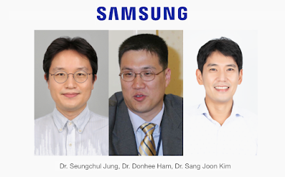
The research was led by Samsung Advanced Institute of Technology (SAIT) in close collaboration with Samsung Electronics Foundry Business and Semiconductor R&D Center. The first author of the paper, Dr. Seungchul Jung, Staff Researcher at SAIT, and the co-corresponding authors Dr. Donhee Ham, Fellow of SAIT and Professor of Harvard University, and Dr. Sang Joon Kim, Vice President of Technology at SAIT, spearheaded the research.

The Samsung Electronics researchers have provided a solution to this issue by an architectural innovation. Concretely, they succeeded in developing an MRAM array chip that demonstrates in-memory computing, by replacing the standard, ‘current-sum’ in-memory computing architecture with a new, ‘resistance sum’ in-memory computing architecture, which addresses the problem of small resistances of individual MRAM devices.

Samsung’s research team subsequently tested the performance of this MRAM in-memory computing chip by running it to perform AI computing. The chip achieved an accuracy of 98% in classification of hand-written digits and a 93% accuracy in detecting faces from scenes.

"In-memory computing draws similarity to the brain in the sense that in the brain, computing also occurs within the network of biological memories, or synapses, the points where neurons touch one another,” said Dr. Seungchul Jung, the first author of the paper. “In fact, while the computing performed by our MRAM network for now has a different purpose from the computing performed by the brain, such solid-state memory network may in the future be used as a platform to mimic the brain by modelling the brain’s synapse connectivity."

https://research.samsung.com/news


Thursday, December 23, 2021

Samsung's new enterprise PCIe 5.0 SSD reads at up to 13,000 MB/sec

Samsung Electronics introduced its next-gen, enterprise SSDs integrating the PCIe 5.0 interface with its own sixth-generation V-NAND.

Samsung said its new PM1743 will feature a sequential read speed of up to 13,000 megabytes per second (MB/s) and a random read speed of 2,500K input/output operations per second (IOPS), offering 1.9x and 1.7x faster speeds over the previous PCIe 4.0-based products. Moreover, write speeds have been elevated significantly, with a sequential write speed of 6,600 MB/s and a random write speed of 250K IOPS, also delivering 1.7x and 1.9x faster speeds, respectively.  In addition, the new SSD can provide improved power efficiency of up to 608 MB/s per watt, which represents about a 30% boost over the previous generation. 

Samsung will offer a variety of capacities from 1.92 terabytes (TB) to 15.36TB in the conventional 2.5-inch form factor, as well as in a 3-inch EDSFF (E3.S) — an increasingly popular SSD form factor designed specifically for next-generation enterprise servers and data centers. 

Samsung also projects that customers deploying 7.5mm EDSFF SSDs will be able to double the storage density in their systems, compared to when the 15mm 2.5-inch form factor is used.

The new SSDs are also expected to be the industry's first PCIe 5.0 SSD with dual-port support.

"For over a decade, Samsung has been delivering SATA, SAS and PCIe-based SSDs that have been recognized for outstanding performance and reliability by leading enterprise server customers including corporations, governments and financial institutions," said Yong Ho Song, Executive Vice President and Head of the Memory Controller Development Team at Samsung Electronics. "The introduction of our PCIe 5.0 SSD, along with PCIe 6.0-based product developments that are underway, will further solidify our technological leadership in the enterprise server market."

"Intel has been working with Samsung to test Samsung's newest PCIe NVMe SSD, the PM1743. Together, we have jointly resolved complicated technical issues encountered with PCIe 5.0 during this initial evaluation period. The performance potential of Gen5 is truly impressive. In the near future, we strongly believe that PCIe Gen5 systems with high-speed NVMe SSDs will have the ability to transform applications such as AI/ML and high-performance databases," said Jim Pappas, Director, Technology Initiatives, Intel Corporation. "Looking ahead, we are confident that Intel and Samsung's continued commitment in industry leadership will provide these and other benefits to our mutual customers."

Mass production is expected in Q1 2022.

https://news.samsung.com/us/samsung-develops-high-performance-pcie-5-ssd-enterprise-servers/

Thursday, December 16, 2021

IBM and Samsung unveil Vertical Transport Field Effect Transistors

IBM and Samsung Electronics unveiled a new class of Vertical Transport Field Effect Transistors (VTFET) - a breakthrough the companies say that could reduce energy usage by 85 percent compared to a scaled fin field-effect transistor (finFET). The design positions the transistors perpendicular to the surface of the chip with a vertical, or up-and-down, current flow. IBM says the vertical positioning allows for greater current flow with less wasted energy. 

The partners have demonstrated a path to scaling beyond nanosheet, implying a path toward manufacturability and further innovation.

Research was carried out at IBM's Albany Nanotech Complex facility.

The companies also announced that Samsung will manufacture IBM's chips at the 5 nm node. These chips are anticipated to be used in IBM's own server platforms. This follows the announcement in 2018 that Samsung would manufacture IBM's 7 nm chips, which became available in the IBM Power10 family of servers earlier this year. The IBM Telum processor, also revealed earlier this year, is similarly manufactured by Samsung using IBM's designs.

https://newsroom.ibm.com/2021-12-14-IBM-and-Samsung-Unveil-Semiconductor-Breakthrough-That-Defies-Conventional-Design

Samsung Foundry targets 3nm in 2022, 2nm in 2025

Samsung Foundry is scheduled to start producing its customers' first 3nm-based chip designs in the first half of 2022, while its second generation of 3nm is expected in 2023.During its 5th annual Samsung Foundry Forum (SFF) 2021 underway this week, Samsung Electronics unveiled plans for continuous process technology migration to 3- and 2-nm based on the company’s Gate-All-Around (GAA) transistor structure.Samsung said its first 3nm GAA process node...


IBM announces 2nm chip breakthrough

IBM unveiled a 2 nanometer semiconductor design and process breakthrough based on a new Gate-All-Around (GAA) nanosheet device architecture. The technology is implemented on a 300 millimeter (mm) wafer built at IBM Research’s semiconductor research facility in Albany, New York.

IBM said it is able to fit 50 billion transistors in a space roughly the size of a fingernail. A 2 nm chip node transistor equates to an approximate 45 percent performance improvement over  7 nm chips. This results in an approximate 75 percent power savings, at the same performance level. 

IBM Research’s Albany lab features one of the most advanced EUV lithography tools in the industry. 

"The IBM innovation reflected in this new 2 nm chip is essential to the entire semiconductor and IT industry," said Darío Gil, SVP and Director of IBM Research. "It is the product of IBM's approach of taking on hard tech challenges and a demonstration of how breakthroughs can result from sustained investments and a collaborative R&D ecosystem approach."


Wednesday, December 15, 2021

Samsung ramps up automotive memory chips for EVs

Samsung Electronics unveiled a portfolio of automotive memory solutions designed for next-generation autonomous electric vehicles. The new lineup includes a 256-gigabyte (GB) PCIe Gen3 NVMe ball grid array (BGA) SSD, 2GB GDDR6 DRAM and 2GB DDR4 DRAM for high-performance infotainment systems, as well as 2GB GDDR6 DRAM and 128GB Universal Flash Storage (UFS) for autonomous driving systems.

The need for high-capacity, high-performance SSDs and graphics DRAM is driven by advanced features in infotainment systems such as high-definition maps, video streaming and 3D gaming, together with the growing use of autonomous driving systems.

Samsung's 256GB BGA SSD controller and firmware are developed in-house for optimized performance, offering a sequential read speed of 2,100 megabytes per second (MB/s) and a sequential write speed of 300MB/s, which are seven and two times faster than today's eMMC, respectively. Furthermore, the 2GB GDDR6 DRAM features up to a 14 gigabit-per-second (Gbps) data rate per pin. Such exceptional speeds and bandwidth will support complex processing of various multimedia applications as well as large amounts of autonomous driving data, contributing to a safer, more dynamic and more convenient driving experience.

"With the recent proliferation of electric vehicles and the rapid advancement of infotainment and autonomous driving systems, the semiconductor automotive platform is facing a paradigm shift. What used to be a seven to eight-year replacement cycle is now being compressed into a three to four-year cycle, and at the same time, performance and capacity requirements are advancing to levels commonly found in servers," said Jinman Han, executive vice president and head of Memory Global Sales & Marketing at Samsung Electronics. "Samsung's reinforced lineup of memory solutions will act as a major catalyst in further accelerating the shift toward the ‘Server on Wheels’ era."