Showing posts with label 3nm. Show all posts

Wednesday, October 6, 2021

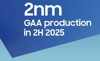
Samsung Foundry targets 3nm in 2022, 2nm in 2025

Samsung Foundry is scheduled to start producing its customers' first 3nm-based chip designs in the first half of 2022, while its second generation of 3nm is expected in 2023.

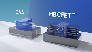
During its 5th annual Samsung Foundry Forum (SFF) 2021 underway this week, Samsung Electronics unveiled plans for continuous process technology migration to 3- and 2-nm based on the company’s Gate-All-Around (GAA) transistor structure.

Samsung said its first 3nm GAA process node utilizing Multi-Bridge-Channel FET (MBCFETTM) will allow up to 35 percent decrease in area, 30 percent higher performance or 50 percent lower power consumption compared to the 5nm process. In addition to power, performance, and area (PPA) improvements, as its process maturity has increased, 3nm’s logic yield is approaching a similar level to the 4nm process, which is currently in mass production.

The 2nm process node with MBCFET is in the early stages of development with mass production in 2025.

“We will increase our overall production capacity and lead the most advanced technologies while taking silicon scaling a step further and continuing technological innovation by application,” said Dr. Siyoung Choi, President and Head of Foundry Business at Samsung Electronics. "Amid further digitalization prompted by the COVID-19 pandemic, our customers and partners will discover the limitless potential of silicon implementation for delivering the right technology at the right time."

Additionally, Samsung is advancing its 14nm process in order to support 3.3V high voltage or flash-type embedded MRAM (eMRAM) which enables increased write speed and density. It will be a great option for applications such as micro controller unit (MCU), IoT and wearables. Samsung’s 8nm radio frequency (RF) platform is expected to expand the company’s leadership in the 5G semiconductor market from sub-6GHz to mmWave applications.

http://news.samsung.com

Tuesday, October 5, 2021

Marvell looks to TSMC's 3nm for custom ASICs

Marvell will use TSMC’s 3nm process technology to offer custom silicon for cloud data center, 5G carrier, automotive and enterprise markets.

Marvell is first to introduce a silicon platform that leverages 3nm process technology, advanced die-to-die interface IP, and TSMC’s advanced 2.5D Chip-on-Wafer-on-Substrate (CoWoS) packaging technology.

“Marvell is proud to be the lead ve3nm3nmndor to offer a 3nm platform for cloud-optimized solutions,” said Sandeep Bharathi, Executive Vice President, Central Engineering, System-on-Chip Group at Marvell. “Our new advanced node platform places Marvell on the leading edge of technology readiness with early Si validation of critical IPs to enable fast time-to-market.”

Marvell's new 3nm multi-chip platform includes two complementary advanced die-to-die interfaces. The first is a flexible extra short reach (XSR) interface for connecting multiple die on a package substrate for applications, like co-packaged optics (CPO) for cloud data centers. 

To address the growing needs for cloud-optimized silicon solutions from leading data center operators, Marvell is also developing an ultra-low power and low-latency parallel die-to-die interface with the highest bandwidth density in the industry. Compatible with emerging Open Compute Project (OCP) standards, the new parallel interface enables high-performance chiplet solutions by connecting multiple silicon devices on an interposer. Both interfaces are also available in 5nm to enable multi-node solutions.

The new platform also incorporates TSMC’s advanced CoWoS packaging technology, empowering continued data infrastructure performance scaling. Marvell said its collaboration with TSMC on CoWoS allows customers to build high-performance solutions for "the most demanding cloud data center applications."

https://www.marvell.com/products/custom-asic.html  


  • Earlier this year, TSMC stated that its 3nm technology (N3) will offer up to 70% logic density gain, up to 15% speed improvement at the same power and up to 30% power reduction at the same speed as compared with N5 technology. N3 is expected to receive multiple customer product tape-outs in 2021. In addition, volume production is targeted in second half of 2022.